Quick Answer
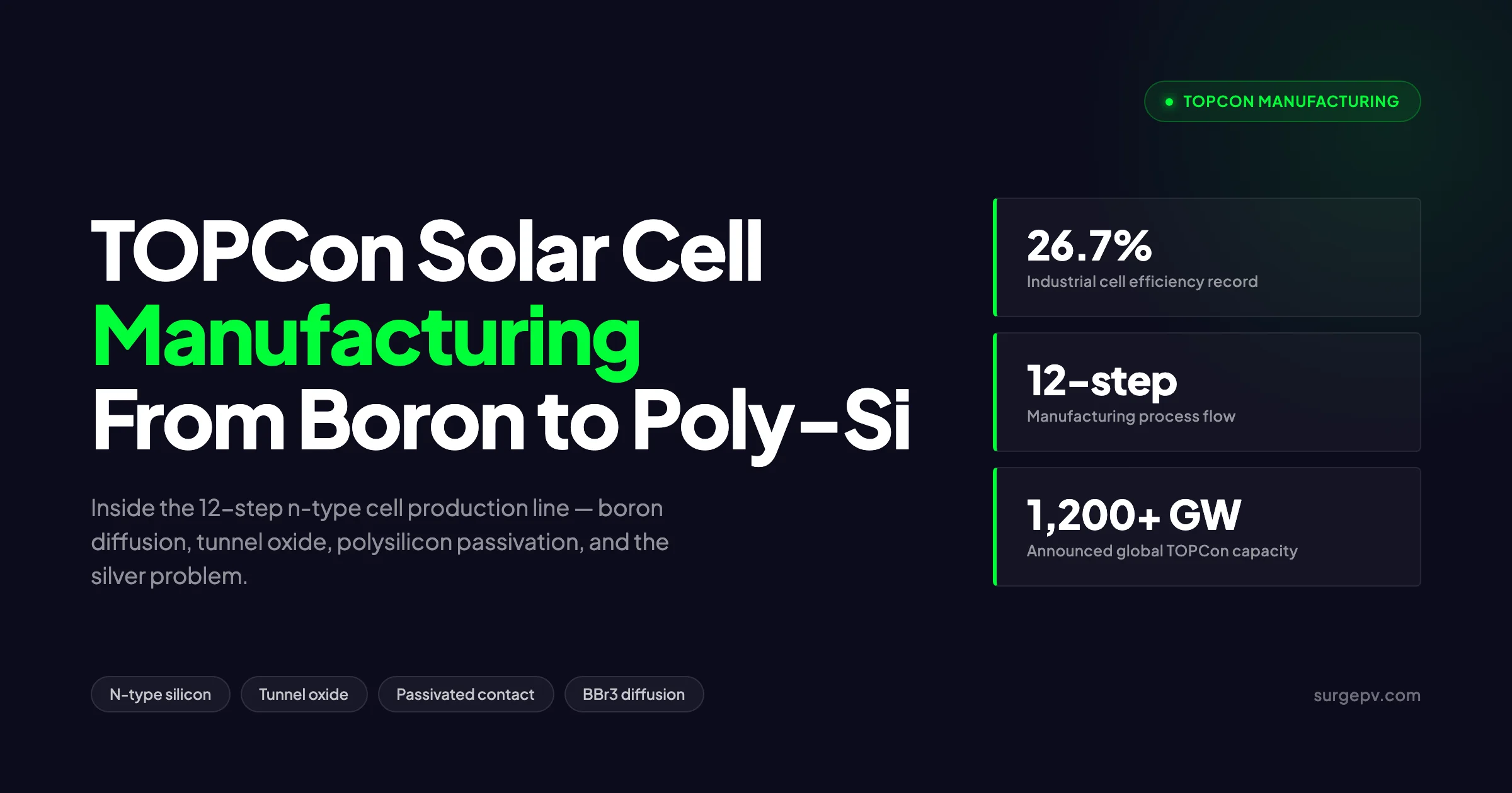
TOPCon manufacturing adds a tunnel oxide layer and polysilicon passivation to standard PERC cells, boosting efficiency to 24–25.5%. Production uses existing PERC lines with €5–10M retrofit investment. Manufacturing cost: $0.08–$0.12/W. TOPCon capacity reached 400 GW in 2025, replacing PERC as the dominant technology.
The factory floor at a 10 GW TOPCon line in Yangzhou runs 24 hours a day. Every 0.7 seconds, a fresh n-type silicon wafer enters the texturing bath. About 90 minutes later, it leaves the firing furnace as a finished 26%-efficient solar cell. Twelve discrete process steps, eighteen pieces of equipment, and a 1.5-nanometer layer of silicon dioxide stand between raw wafer and shippable product. For more on this topic, see TOPCon vs HJT vs Perovskite Solar Panels.
TOPCon manufacturing adds a tunnel oxide layer and polysilicon passivation to standard PERC cells, boosting efficiency to 24–25.5%. Production uses existing PERC lines with €5–10M retrofit investment. Manufacturing cost: $0.08–$0.12/W.
TOPCon manufacturing adds a tunnel oxide layer and polysilicon passivation to standard PERC cells, boosting efficiency to 24–25.5%. Production uses existing PERC lines with €5–10M retrofit investment. Manufacturing cost: $0.08–$0.12/W. TOPCon capacity reached 400 GW in 2025, replacing PERC as the dominant technology.
That 1.5-nanometer layer is the whole story. It is what TOPCon means — Tunnel Oxide Passivated Contact — and it is the reason TOPCon has taken 85% of global solar cell production in 2025, according to CRU’s solar module tracker. For Global-specific compliance details, see Global net-metering-by-country. For Global-specific compliance details, see Global solar-permitting-speed-by-country.
Quick Answer
TOPCon solar cell manufacturing is a 12-step process for building n-type silicon cells. The cell uses a boron-diffused p+ emitter on the front and a rear stack of ultra-thin tunnel oxide plus doped polysilicon. This combination passivates the rear contact, reaches 26% cell efficiency in mass production, and powers the modules that ship 670W+ at the factory gate in 2026.
This guide walks through every step of the TOPCon production line — what happens, why, the equipment used, and the tradeoffs between competing process routes. Engineers can use it as a reference. Buyers can use it to understand what they are paying for in solar design software when they import the latest TOPCon module datasheets.
You will learn:
- How the n-type wafer is prepared and textured
- The chemistry of boron diffusion and why it controls cell efficiency
- How the tunnel oxide is grown and what makes it work
- The hard tradeoff between LPCVD and PECVD polysilicon
- Front and rear passivation chemistry
- Screen-printing and the silver consumption problem
- Co-firing, regeneration, and quality control
- 2026 cost, capex, and capacity data
Latest Updates: TOPCon Manufacturing in 2026
TOPCon mass production has shifted three times in the last 18 months. Silver consumption, in-situ doping, and selective emitter laser doping are now the active battlegrounds.
| Date | Update | Impact |
|---|---|---|
| Feb 2026 | JinkoSolar / NIMTE certify 26.66% industrial TOPCon cell | Highest industrial efficiency for a mass-produced silicon cell |
| Feb 2026 | Trina Solar hits 32.6% on full-size perovskite/TOPCon tandem | Confirms TOPCon as the bottom cell for next-gen tandems |
| Apr 2026 | Fraunhofer ISE demonstrates 1.1 mg/Wp silver TOPCon via nickel-copper plating | Cuts silver from ~10-12 mg/Wp to ~1 mg/Wp |
| May 2026 | Jolywood starts mass production of low-silver “Namic” TOPCon cells | First commercial low-silver TOPCon, over 27% efficiency |
| Q1 2026 | JinkoSolar, JA Solar, Trina, Tongwei each pass 80 GW annual TOPCon capacity | Top four account for over 50% of global shipments |
The biggest open question of 2026 is whether PECVD overtakes LPCVD as the dominant polysilicon deposition method. The ITRPV roadmap projects PECVD share rising from under 20% in 2022 to nearly 50% by 2027.
What Is a TOPCon Solar Cell?
A TOPCon cell is an n-type monocrystalline silicon solar cell with a passivated contact on the rear. The rear contact is what makes it different.
In a standard PERC cell, the metal rear electrode touches the silicon directly through openings in a dielectric layer. Every place metal touches silicon, electrons and holes recombine. This wastes about 30 mV of open-circuit voltage.
A TOPCon cell solves this by inserting two layers between the silicon and the metal:
- Tunnel oxide — a 1.2 to 1.6 nm film of SiO2 grown directly on the silicon
- Polysilicon — a 100 to 150 nm layer of phosphorus-doped polycrystalline silicon
The tunnel oxide is thin enough that electrons quantum-tunnel through it. The doped polysilicon attracts electrons (because it is n+) and repels holes. The result is a contact that lets electrons out efficiently but blocks holes from recombining at the metal.
The full cell stack from front to back in 2026:
| Layer | Material | Thickness | Function |
|---|---|---|---|
| Front contact | Silver paste fingers | 12-15 micron | Electron collection |
| ARC | SiNx | 75-80 nm | Anti-reflection |
| Front passivation | AlOx | 4-8 nm | p+ surface passivation |
| Emitter | Boron-diffused p+ Si | 0.3-0.5 micron | p-n junction |
| Bulk | n-type c-Si wafer | 130-160 micron | Photon absorption |
| Tunnel oxide | SiO2 | 1.2-1.6 nm | Passivated contact |
| Poly-Si layer | n+ doped polysilicon | 100-150 nm | Carrier selectivity |
| Rear ARC | SiNx | 70-90 nm | Optical reflection |
| Rear contact | Silver-aluminum paste | 8-12 micron | Electron extraction |
Why TOPCon Replaced PERC
PERC dominated solar manufacturing from 2015 to 2023. By the end of 2025, it was below 5% of new production.
The shift happened because three things lined up:
- Higher efficiency ceiling: PERC tops out at about 23.5% cell efficiency. TOPCon mass-production cells already exceed 26%, with a roadmap toward 27%.
- Drop-in retrofit: Most PERC lines were converted to TOPCon by adding 4-5 new tools rather than building new fabs. Capex for retrofit ran around RMB 50-80 million per GW, against RMB 250 million for a greenfield TOPCon line.
- Lower temperature coefficient: TOPCon modules lose -0.29%/C versus -0.34%/C for PERC. Over a hot rooftop year in Arizona, that is roughly 1.5% more energy yield.
The first TOPCon mass-production line started at Jolywood in 2019. By 2026, TOPCon is the default for new utility-scale solar software databases — Tier 1 manufacturers ship more than 80 GW per year each. Installers running commercial solar projects now specify TOPCon by default; residential solar catalogs are following.
The 12-Step TOPCon Manufacturing Process
Here is the full process flow used in a 2026 mass-production line. Cycle time from wafer-in to cell-out is roughly 90-120 minutes.
| Step | Process | Tool | Time | Function |
|---|---|---|---|---|
| 1 | Wafer texturing | Wet bench (KOH) | 5-8 min | Pyramid formation |
| 2 | Boron diffusion | Tube furnace (BBr3/BCl3) | 120 min | Front p+ emitter |
| 3 | BSG removal | Inline wet etch | 2 min | Strip borosilicate glass |
| 4 | Tunnel oxide growth | Tube furnace or PECVD | 5-15 min | 1.5 nm SiO2 |
| 5 | Poly-Si deposition | LPCVD or PECVD | 30-90 min | 100-150 nm a-Si |
| 6 | Phosphorus doping | POCl3 furnace or in-situ | 60 min | n+ doping of poly-Si |
| 7 | Wraparound removal | Wet etch (BOE+KOH) | 3 min | Remove parasitic poly-Si |
| 8 | Edge isolation | Laser or wet etch | under 1 min | Isolate front from rear |
| 9 | ARC deposition | PECVD (SiNx, AlOx) | 5-10 min | Anti-reflection, passivation |
| 10 | SE laser doping | UV/green laser | under 1 min | Selective boron emitter |
| 11 | Metallization | Screen printer | 3-5 min | Silver paste fingers |
| 12 | Co-firing | Belt furnace (~800C) | 5 min | Ohmic contact, hydrogen activation |
Each step has subtle process windows. Miss the boron diffusion temperature by 20C and the emitter sheet resistance drifts. Get the tunnel oxide 0.3 nm too thick and tunneling probability drops by 50%. Let the firing peak run 30C high and silver fingers punch through the SiNx and short the cell.
Step 1: Wafer Texturing
The starting wafer is an n-type Czochralski-grown monocrystalline silicon wafer, typically 182 or 210 mm square. Wafer thickness in 2026 is 130-150 micron, down from 180 micron in 2021.
The wafer comes from wire-saw cutting with surface damage 2-5 micron deep. Texturing serves two purposes:
- Remove saw damage
- Form pyramids that trap incoming light
The bath chemistry is hot potassium hydroxide (KOH) at 70-85C plus an isopropanol or proprietary additive (IPA-free additives are now standard). The KOH etches silicon anisotropically — it attacks the (100) crystal face about 100 times faster than the (111) face. This leaves behind upright pyramids with (111) sidewalls.
Target pyramid size in 2026 lines is 1-3 micron, smaller than the 5-10 micron pyramids of PERC era. Smaller pyramids cut the surface area where boron will later diffuse, which lowers j0e (emitter saturation current).
After texturing, the wafer is RCA-cleaned in HCl-based and HF baths to remove metal contamination and native oxide.
Step 2: Boron Diffusion — The Heart of TOPCon
Boron diffusion forms the front p+ emitter. This is the most thermally demanding step in the process and the single biggest lever on cell efficiency.
The standard industrial process is tube furnace diffusion using boron tribromide (BBr3) as the precursor. A typical recipe:
- Load 1,500-2,000 wafers vertically in a quartz boat
- Ramp to 950-980C under N2
- Inject BBr3 vapor mixed with O2 for 20-40 minutes
- Drive-in at higher temperature for 30-60 minutes
- Post-oxidation under O2 to seal the surface
- Cycle time: about 2 hours total
The chemistry inside the tube is straightforward. BBr3 reacts with O2 to form B2O3 and Br2 vapor. The B2O3 reacts with silicon at the wafer surface, depositing boron and forming SiO2. The B2O3 plus SiO2 mixture is the borosilicate glass (BSG) layer on the surface. Boron atoms then diffuse from the BSG into the silicon to form the p+ emitter.
The process targets these parameters per recent Fraunhofer ISE work:
- Sheet resistance: 150-200 ohm/sq
- Junction depth: 0.3-0.5 micron
- Surface peak concentration: 1-3 × 10^19 cm^-3
- j0e (under SiNx passivation): 15-30 fA/cm^2
- Uniformity across boat: under 5% standard deviation
A boron-rich layer (BRL) forms during diffusion if oxygen flow is wrong. This layer causes lifetime degradation and must be removed in step 3.
The alternative precursor is boron trichloride (BCl3), which is cheaper and easier to handle but harder to control for low sheet resistance. Some Tier 1 lines use BCl3 plus spin-on borosilicate or PECVD-deposited BSG for selective emitter formation.
Pro Tip for Process Engineers
Watch the O2 flow rate during boron diffusion. Too little O2 grows a thin BSG that won’t protect the emitter during downstream wet etches. Too much O2 builds a thick boron-rich layer that recombines carriers. The window for 2026 high-efficiency cells is 200-400 sccm O2 at 980C.
Step 3: BSG and Rear Emitter Removal
After diffusion, both wafer faces are covered with BSG. The rear face also has a parasitic p+ layer from BBr3 wraparound during diffusion. Both must go.
The standard tool is an inline wet bench with three baths:
- HF/HCl bath — strips rear BSG only (single-side, liquid carried on top rollers)
- KOH bath — removes the rear emitter, about 5 micron of silicon
- HF rinse — removes residual oxide
The front BSG is preserved through this step. It protects the front emitter from the KOH attack and is removed later.
Step 4: Tunnel Oxide Growth
This is the layer that makes TOPCon what it is. The target is 1.2 to 1.6 nm of SiO2 on the rear surface — about 4-5 atomic layers.
Three deposition routes are used industrially:
| Method | Temperature | Quality | Throughput | Used by |
|---|---|---|---|---|
| Thermal oxidation (dry O2) | 600-700C | Excellent | Low | JinkoSolar (LPCVD lines) |
| Wet chemical (HNO3) | 80-90C | Good | High | JA Solar, Trina |
| Plasma-assisted (N2O plasma) | 350-450C | Good | High | New PECVD lines |
The oxide cannot be too thick (electrons stop tunneling above about 2 nm) or too thin (chemical passivation breaks down below about 0.8 nm). The Goldilocks zone is narrow.
Wet chemical oxidation has won most new capacity because it integrates cleanly with the wet bench used for BSG removal. Heat-up time is zero, throughput is high, and oxide uniformity is excellent across 210 mm wafers.
Step 5: Polysilicon Deposition — The LPCVD vs PECVD War
The polysilicon layer is 100-150 nm of amorphous silicon, later crystallized to polysilicon during annealing. This is where the manufacturing routes split.
LPCVD route
- Temperature: 520C
- Pressure: 250 mTorr
- Precursor: SiH4
- Throughput: 100-150 wafers per tube per cycle (3-4 hours)
- Coats both faces of the wafer
PECVD route
- Temperature: 300C
- Pressure: 150 mTorr (RF plasma)
- Precursor: SiH4 plus PH3 (in-situ phosphorus)
- Throughput: 20 times faster than LPCVD
- Coats only the rear face
The performance difference is real. PECVD allows in-situ phosphorus doping, which eliminates a separate POCl3 step (step 6). It also avoids parasitic poly-Si on the front face, cutting the wraparound removal step.
But PECVD has problems:
- Ion bombardment damage: RF plasma ions strike the tunnel oxide during deposition. This creates interface defect states that can cost 40-50 mV of implied open-circuit voltage if not controlled, per published Fraunhofer ISE work.
- Blistering: Hydrogen trapped in PECVD-deposited a-Si releases during high-temperature anneal. The film blisters off the wafer. Solving this needs careful staging of deposition power and pulse duty cycle.
- Thinner optimal tunnel oxide: PECVD lines need about 0.8 nm oxide rather than about 1.5 nm, which tightens the process window.
The industry workaround is a dual-layer PECVD recipe: deposit an intrinsic a-Si(i) buffer first at low plasma power to protect the tunnel oxide, then deposit the heavily doped a-Si(n+) on top. Recent cell results show 23.3% efficiency from this route at Fraunhofer ISE, matching LPCVD performance.
Why LPCVD Is Losing to PECVD Even Though It Makes Better Cells
The industry conventional wisdom says LPCVD makes the best TOPCon cells. The data backs this up — LPCVD lines hit 26.5% cell efficiency more reliably than PECVD lines.
So why is PECVD winning new capacity decisions?
Three reasons that have nothing to do with cell quality:
Throughput economics. A PECVD tube deposits 100-150 nm of poly-Si in 3-5 minutes. An LPCVD tube takes 60-90 minutes for the same thickness. To match throughput, a fab needs roughly 6-8 LPCVD tubes per GW versus 1-2 PECVD tubes. That difference dominates the capex calculation, even though each PECVD tube is more expensive per unit.
The wraparound elimination. LPCVD coats both wafer faces. This means an extra wet etch step to remove the front poly-Si, plus careful single-side processing through 3-4 downstream tools. PECVD only coats the rear. The elimination of wraparound removal saves $0.003-0.005 per cell — small per cell but $30-50 million per year on a 10 GW line.
In-situ phosphorus doping. With PECVD, the dopant goes in during deposition. With LPCVD, a separate POCl3 furnace step is needed (step 6). Eliminating one furnace tool per GW saves capex of roughly $5-8 million.
The honest answer to the LPCVD vs PECVD question in 2026: LPCVD makes 0.1-0.2% better cells. PECVD makes them 5-10% cheaper. In a market with cell price of $0.08/W, 5-10% cost beats 0.1-0.2% efficiency. So PECVD is winning new capacity, while LPCVD persists in the highest-end lines where binned efficiency matters more than cell cost.
Step 6: Phosphorus Doping of the Polysilicon
For LPCVD-deposited poly-Si, this is a separate step in a POCl3 tube furnace. For PECVD lines with in-situ doping, this step is skipped.
The POCl3 process:
- Temperature: 800-850C
- Time: 40-60 minutes
- Precursor: POCl3 vapor plus O2
- Target sheet resistance of poly-Si: 60-100 ohm/sq
The chemistry mirrors boron diffusion in step 2. POCl3 reacts with O2 to form P2O5, which deposits as phosphosilicate glass (PSG) on the surface. Phosphorus diffuses from PSG into the poly-Si during the high-temperature step.
The PSG layer is removed downstream during the wraparound-removal etch.
Step 7: Wraparound Removal
LPCVD-deposited poly-Si covers the front face of the wafer on top of the BSG. This parasitic layer must be removed without damaging the front emitter.
The standard tool is a single-side wet etch:
- BOE bath (buffered HF) — removes the front BSG, exposing front poly-Si
- KOH bath — etches the exposed front poly-Si (KOH attacks textured silicon faster than thermal SiO2)
- HF bath — strips residual oxide
The rear poly-Si is protected by riding the wafer on top of a liquid layer, with the etchant only contacting the front face.
For PECVD lines, only the wafer edges have parasitic poly-Si. A simpler edge-only laser ablation or shorter wet etch is used.
Step 8: Edge Isolation
The front emitter (p+) and the rear poly-Si (n+) must be electrically isolated. If they touch around the wafer edge, the cell shunts and shorts to zero.
Two routes:
- Laser edge isolation: A UV or green laser scribes a 50 micron wide groove around the wafer perimeter, cutting through the front emitter to the bulk silicon.
- Wet etch edge isolation: Done together with the wraparound removal step in the same wet bench.
Modern 2026 lines use laser for tighter dimensional control and lower kerf loss.
Step 9: Anti-Reflection and Passivation Coating
The front face gets two layers; the rear gets one (over the poly-Si).
Front side, in order:
- AlOx (aluminum oxide) — 4-8 nm deposited by ALD (atomic layer deposition). The fixed negative charges in AlOx field-passivate the p+ emitter.
- SiNx (silicon nitride) — 75-80 nm deposited by PECVD. Acts as the anti-reflection coating tuned to peak reflection minimum at about 600 nm. Also serves as a hydrogen reservoir for firing.
Rear side:
- SiNx — 70-90 nm by PECVD. Acts as a rear optical mirror and dielectric. Hydrogen in this layer passivates the poly-Si/c-Si interface during firing.
ALD is a slow process (1-2 nm per minute). For 200+ MW per tool per year, modern lines use spatial ALD or batch ALD chambers running 12-24 wafers simultaneously.
Step 10: Selective Emitter Laser Doping
To squeeze 0.2-0.4% more efficiency, most 2026 TOPCon lines add a selective emitter (SE) step.
A green or UV laser scans the wafer surface only along the locations where front silver fingers will land. The laser briefly melts the silicon (less than a microsecond per pulse). The boron in the borosilicate glass — which was preserved through step 3 — diffuses rapidly into the molten silicon, creating a heavily doped p++ zone under the future contact.
Result: the silicon under the silver fingers has high boron concentration (good for low contact resistance), while the silicon between fingers stays lightly doped (good for low recombination and high blue response).
The efficiency gain is real: industrial data shows 0.2-0.3% absolute efficiency gain from SE laser doping.
Design Solar Projects With 2026 TOPCon Modules
SurgePV’s library auto-updates with the latest 670W+ TOPCon modules from JinkoSolar, JA Solar, Trina, Tongwei, and 30+ other Tier 1 manufacturers. Simulate yield, run shadow analysis, and generate proposals with accurate temperature coefficients and bifacial gain.
Book a DemoNo commitment required · 20 minutes · Live project walkthrough
Read Bifacial Solar Panel Design Guide for a complete walkthrough.
Step 11: Screen-Printing Metallization
Screen printing applies the front and rear metal contacts. The cell is loaded onto a vacuum chuck, a stencil with the finger and busbar pattern is positioned above, and silver paste is squeegeed through the openings.
Front side:
- Material: silver paste (Ag content over 90%, glass frit and organic binders for the rest)
- Finger count: 16-20 busbars (zero-busbar with 26-30 fingers becoming standard in 2026)
- Finger width: 15-25 micron after firing
- Paste consumption: 60-80 mg per cell
Rear side:
- Material: silver-aluminum paste for contact regions, full Ag paste for busbars
- Coverage: 5-15% of rear area in fingers, rest is exposed SiNx (for bifacial operation)
- Paste consumption: 80-120 mg per cell
Total silver consumption per TOPCon cell in 2026 is 10-12 mg/Wp. This is roughly twice what a PERC cell needs because TOPCon’s higher voltage requires more conductive fingers and the rear contact also uses silver.
Silver paste makes up about 30% of total cell cost. The cost pressure has driven two innovations:
- Low-silver TOPCon (Jolywood Namic): Started mass production in May 2026. Partial substitution of silver with aluminum paste in the metallization. The Namic architecture prevents aluminum diffusion into the silicon. Result: lower paste cost, over 27% efficiency.
- Plated copper TOPCon (Fraunhofer ISE): Demonstrated 1.1 mg/Wp silver by replacing screen-printed silver with electroplated nickel/copper/silver fingers. Commercial deployment expected within 2-3 years.
For a deeper cost sensitivity analysis of cell costs and final installed system economics, see our blog post on solar panel ROI in Italy. Also see: solar panel ROI in Italy.
Step 12: Co-Firing
The printed cell goes into an infrared belt furnace. The belt moves at 5-7 meters per minute through five temperature zones:
| Zone | Temperature | Purpose |
|---|---|---|
| Pre-heat | 150-300C | Burn off paste organics |
| Burn-out | 400-500C | Decompose binders |
| Ramp | 600-700C | Approach firing peak |
| Peak | 780-830C | Form ohmic contacts, activate hydrogen |
| Cool | 300C | Controlled cooling |
The peak temperature does two critical things:
- The glass frit in the silver paste etches through the SiNx and contacts the silicon directly, forming ohmic contacts
- Hydrogen in the SiNx layers diffuses to the silicon interfaces, passivating dangling bonds and defects
Peak temperature must be tightly controlled. Too low: contacts are resistive (high series resistance, low fill factor). Too high: silver punches deep into the silicon (high recombination, low Voc). The window in 2026 lines is plus or minus 5C.
After firing, cells get a Light and elevated Temperature Induced Degradation (LeTID) regeneration step: 5-10 minutes under intense light at 70-80C. This stabilizes the boron-oxygen defect complexes that would otherwise cause 1-2% efficiency loss over the first 100 hours of field exposure.
Quality Control and Binning
Every cell is electrically tested before packing. A 2026 production tester runs through:
- I-V curve under standard test conditions (1000 W/m^2, 25C, AM1.5G spectrum)
- Electroluminescence imaging — looks for cracks, finger breaks, and process defects
- Photoluminescence (sometimes) — looks for bulk lifetime variations
Cells are binned by power output, typically in 0.05 W increments. A 2026 mass-production TOPCon cell delivers 7.2 to 7.4 watts on a 182 mm wafer (M10 format) or 9.5 to 9.8 watts on a 210 mm wafer (G12 format).
Yield in a well-tuned line is 96-98% — i.e., 2-4% of cells fail electrical or visual QC and are rejected.
TOPCon Cost Breakdown 2026
Total cell production cost in 2026 for a Tier 1 manufacturer:
| Cost Component | $/W | % of Total |
|---|---|---|
| Wafer (n-type c-Si) | $0.030 | 38% |
| Silver paste (10-12 mg/Wp) | $0.018 | 23% |
| Other consumables (gases, chemicals) | $0.008 | 10% |
| Electricity | $0.006 | 8% |
| Labor | $0.004 | 5% |
| Equipment depreciation | $0.008 | 10% |
| Yield loss plus reject | $0.005 | 6% |
| Total cell cost | $0.079 | 100% |
Module assembly (glass, EVA, backsheet, frame, junction box, ribbon) adds another $0.08-0.10/W, bringing total module cost to $0.16-0.18/W ex-factory.
The single biggest cost lever is silver. Cutting silver from 11 mg/Wp to 1 mg/Wp would knock $0.015 off cell cost, or roughly 20%. This is why every Tier 1 manufacturer has a silver-reduction roadmap. For project developers running solar proposal software economics, this means 10-15% drops in TOPCon module ASP are baked in for 2027-2028.
Capex per GW
Building a new 10 GW TOPCon cell line in 2026 requires about $250-300 million in equipment, or RMB 250 million per GW.
| Equipment | Capex per GW (USD M) |
|---|---|
| Texturing wet benches | 1.5 |
| Boron diffusion tubes | 4.0 |
| BSG removal wet bench | 1.5 |
| Tunnel oxide plus poly-Si (LPCVD route) | 12.0 |
| Tunnel oxide plus poly-Si (PECVD route) | 7.0 |
| Phosphorus doping (skipped for PECVD in-situ) | 2.0 |
| Wraparound removal | 1.5 |
| Edge isolation laser | 0.5 |
| AlOx ALD | 2.5 |
| SiNx PECVD | 3.0 |
| SE laser doping | 1.0 |
| Screen printers | 1.5 |
| Co-firing furnaces | 1.5 |
| Cell testing and sorting | 1.0 |
| Automation and material handling | 2.5 |
| Total | 27-32 |
A 10 GW line costs $270-320 million. Greenfield TOPCon today is roughly 50% more capex-intensive than greenfield PERC was at peak in 2020, but 2-3x cheaper than greenfield HJT.
TOPCon Capacity by Manufacturer
The top 10 TOPCon manufacturers in 2026 by announced capacity:
| Manufacturer | TOPCon Capacity (GW) | Notable Products |
|---|---|---|
| JinkoSolar | 95+ | Tiger Neo 3.0 (650-670W) |
| JA Solar | 85+ | DeepBlue 4.0 Pro |
| Trina Solar | 80+ | Vertex N |
| Tongwei | 80+ | TNC |
| Canadian Solar | 50+ | TOPHiKu7 |
| Risen Energy | 45+ | Hyper-ion |
| Jolywood | 35+ | Niwa Star (Namic low-Ag) |
| Astronergy | 35+ | ASTRO N7s |
| LONGi (legacy TOPCon) | 30+ | Hi-MO N (being phased out for BC) |
| GCL System Integration | 25+ | GCL-M10/G12 N |
LONGi is the notable exception — the company has pivoted to back-contact (BC) cells, with 66% of its Q1 2026 shipments being BC. Other Tier 1 players are doubling down on TOPCon plus tandem TOPCon/perovskite for the next-generation product.
TOPCon-Specific Reliability Challenges
Three failure modes are unique to TOPCon and need active management.
PID-p (Positive Potential Induced Degradation)
Standard PID hits PERC modules at negative voltage. TOPCon modules can also degrade at positive voltage — PID-p. The mechanism involves sodium ion migration from the front glass through the AlOx/SiNx into the boron emitter, where it neutralizes positive charges.
Mitigation: ALD-deposited AlOx with optimized thickness, tighter glass quality control, and module-level testing to IEC 62804-1.
UV Degradation
TOPCon’s high-quality passivation is partially undone by UV light exposure. The mechanism is UV-induced break of Si-H bonds at the AlOx/Si interface. Field data shows 1-3% efficiency loss in the first year before the cell stabilizes.
Mitigation: UV-cut EVA encapsulant, optimized AlOx thickness, hydrogen-rich firing recipes.
Silver Migration
Under hot-humid conditions, silver in the front fingers can migrate, increasing series resistance over time. This becomes a larger problem as silver consumption is cut and finger cross-sections shrink.
Mitigation: silver-aluminum paste with corrosion inhibitors, edge sealants, and IEC 61215 damp heat testing extended to 3,000 hours for premium-tier products.
What Comes After TOPCon
TOPCon will dominate 2026-2028, but the next platform is already being commercialized. Three directions:
- TOPCon plus perovskite tandems: Trina has demonstrated 32.6% on full-size modules in February 2026, working with Oxford PV. Mass production targeted for 2027.
- All-back-contact TOPCon (TBC): Moves the front fingers to the rear, gaining about 1% efficiency. JinkoSolar and JA Solar both have pilot lines. Capex is 1.3-1.5x higher than standard TOPCon.
- Plated copper TOPCon: Replaces 90% of silver with electroplated copper. Fraunhofer ISE pilot demonstrated 24% cell efficiency at 1.1 mg/Wp silver. Commercial production expected 2027-2028.
For installers and project developers, this means the 670W TOPCon modules of 2026 will be matched by 720W TOPCon/perovskite tandems by 2028. The change in solar shadow analysis software requirements is minor — same form factor, same temperature coefficient, just more watts per square meter.
Conclusion: Three Actions to Take
- For installers: Switch your default module database to 2026 TOPCon products. Modules below 24% efficiency are now bottom-of-tier. Use solar design software that auto-updates module data so you do not lock in obsolete specs in proposals.
- For procurement: Demand IEC 62804-1 (PID-p) and IEC 61215 ED.4 test results. The cheap end of the TOPCon market has unresolved PID-p exposure that will not show up for 2-3 years in the field.
- For developers running financial models: Recalculate degradation curves. TOPCon’s first-year light-induced degradation is different from PERC (better long-term, worse first 100 hours). Use the generation and financial tool to model TOPCon-specific degradation profiles.
Frequently Asked Questions
What is TOPCon solar cell manufacturing?
TOPCon (Tunnel Oxide Passivated Contact) manufacturing is a 12-step process that builds a high-efficiency n-type silicon solar cell. The signature steps are boron diffusion to form the front p+ emitter and the deposition of an ultra-thin (~1.5 nm) tunnel oxide plus a doped polysilicon layer on the rear. This stack passivates the rear contact and pushes commercial cell efficiency above 25%.
Why is TOPCon better than PERC?
TOPCon uses an n-type wafer and a rear passivated contact, which cuts recombination losses. Commercial TOPCon modules reach 24.5% efficiency in 2026, against about 22% for PERC. TOPCon also has a lower temperature coefficient and better low-light response. The technology won 85% of global cell production in 2025, per CRU.
What is the role of the tunnel oxide in a TOPCon cell?
The tunnel oxide is a 1.2 to 1.6 nm layer of SiO2 between the silicon wafer and the doped polysilicon. It is thin enough for electrons to tunnel through but thick enough to chemically passivate the silicon surface. This blocks minority carriers and lets majority carriers pass, which is the trick that gives TOPCon its high open-circuit voltage.
What is the difference between LPCVD and PECVD in TOPCon manufacturing?
LPCVD (Low Pressure Chemical Vapor Deposition) deposits polysilicon at about 520C on both wafer faces and gives mature, high-quality passivation. PECVD (Plasma Enhanced Chemical Vapor Deposition) runs at about 300C, deposits 20 times faster, and only coats one side, but it can damage the tunnel oxide through ion bombardment. PECVD share is forecast to hit nearly 50% of TOPCon lines by 2027.
How much silver does a TOPCon cell use?
A standard TOPCon cell uses 10 to 12 milligrams of silver per watt-peak in 2026 — roughly twice as much as a PERC cell. This silver consumption is the single biggest variable cost in TOPCon production. Fraunhofer ISE has demonstrated a nickel-copper plating route that cuts silver use to 1.1 mg/Wp, and commercial rollout is expected within 2 to 3 years.
What is the cell efficiency record for TOPCon?
JinkoSolar set a 27.79% conversion efficiency record for a full-size TOPCon cell in 2025. The certified industrial record stands at 26.66%, set by NIMTE and JinkoSolar in 2026. Commercial mass-production cells typically run at 25.5 to 26%, with modules at 23 to 24.5%.
How long does it take to manufacture a TOPCon cell?
Total cycle time from wafer-in to cell-out is 90 to 120 minutes on a 2026 mass-production line. The longest individual step is boron diffusion at about 2 hours per tube load, but with 6-10 tubes running in parallel per GW, throughput is roughly 6 cells per second across the full line.
Can a PERC factory be upgraded to TOPCon?
Yes — and most TOPCon capacity in 2024-2025 came from PERC retrofits rather than greenfield builds. The retrofit adds 4-5 new tools: a boron diffusion tube, a tunnel oxide plus polysilicon deposition tool, a phosphorus doping tool (for LPCVD route), and a wraparound removal wet bench. Retrofit capex runs RMB 50-80 million per GW, against RMB 250 million for a greenfield TOPCon line.
What is the typical TOPCon module efficiency in 2026?
Commercial TOPCon modules in 2026 ship at 22.5 to 24.5% efficiency, with median around 23%. Top-tier products from JinkoSolar (Tiger Neo 3.0), JA Solar (DeepBlue 4.0 Pro), and Trina (Vertex N) hit 24.0 to 24.5% on bifacial 670W+ modules. This is up from 22% commercial TOPCon in 2023 and 20% commercial PERC in 2020.