Quick Answer
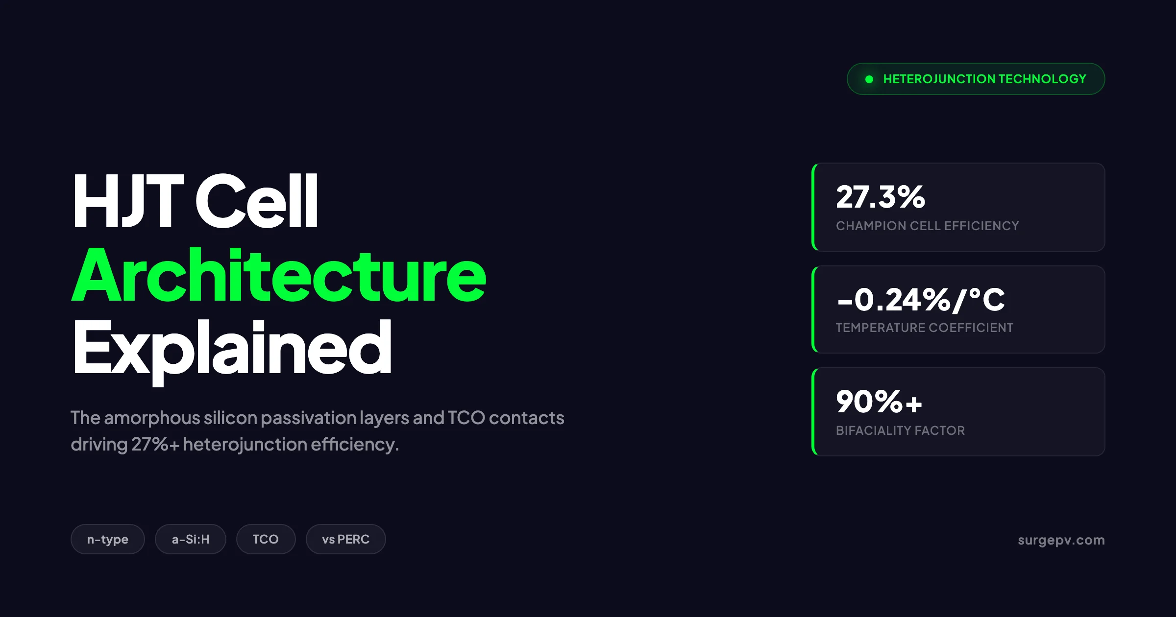
Source HJT cell world record. 27.3% (LONGi HBC). ISFH certification, May 2024 HJT cell (non-BC) record. 27.08% (Trina Solar). Commercial datasheets Silver consumption per cell. 75 mg (2025 average). CPIA 1 GW HJT line capex. ~$61 million. Industry reports Projected HJT market share by 2031. ~20% of n-type production.
Walk into any HJT production line and the first thing you notice is what is missing. There is no high-temperature firing furnace. No 800°C diffusion step. The whole cell stack is built at around 200°C, with the most demanding step being a plasma-enhanced chemical vapor deposition tool that lays down films a few nanometers thick. That single fact — low-temperature processing — is the architectural decision that lets HJT cells deliver 27.3% efficiency in the lab and a temperature coefficient of –0.24%/°C in the field. Every other advantage flows from it. This guide breaks down the HJT cell stack layer by layer, explains why each layer is engineered the way it is, and shows why heterojunction beats PERC on every metric except cost in 2026.
Source HJT cell world record. 27.3% (LONGi HBC). ISFH certification, May 2024 HJT cell (non-BC) record.
TL;DR — HJT Cell Architecture in 2026
HJT sandwiches an n-type crystalline silicon wafer between two intrinsic amorphous silicon (a-Si:H) passivation layers, with doped a-Si:H emitter and back-surface-field layers, transparent conductive oxide contacts, and a screen-printed silver or silver-copper grid. The symmetric structure delivers bifaciality factors above 90%, temperature coefficients near –0.24%/°C, and module efficiency of 24–26% in mass production. LONGi pushed the lab record to 27.3% in 2024 and 28.13% with HIBC in 2026. The trade-off is capital cost — roughly $61 million per GW of capacity — but the resulting kWh per installed watt is the highest of any commercial silicon technology.
Read Bifacial Solar Panel Design Guide for a complete walkthrough.
What this guide covers:
- The complete HJT cell stack, layer by layer, with the physics behind each film
- Why the n-type wafer matters and how it eliminates light-induced degradation
- How amorphous silicon passivation drives open-circuit voltage above 750 mV
- The role of transparent conductive oxide and why indium supply is a bottleneck
- HJT manufacturing flow: four steps, low-temperature processing, capital cost
- Real efficiency data: commercial modules, lab records, and 2026 milestones
- HJT vs PERC vs TOPCon: where each architecture wins and why
- Major manufacturers and 2026 product specifications
Latest Updates: HJT Technology in 2026
The HJT roadmap moved faster in the last 18 months than in the previous five years. Here is the current state as of May 2026.
| Milestone | Value (2026) | Source |
|---|---|---|
| HJT cell world record | 27.3% (LONGi HBC) | ISFH certification, May 2024 |
| HJT cell (non-BC) record | 27.08% (Trina Solar) | December 2024 |
| HIBC cell record | 28.13% (LONGi) | ISFH 2026 |
| Mass-production module efficiency | 24–26% | Multiple manufacturers |
| Best commercial module | 26.07% (monofacial) | Risen Hyper-ion |
| Temperature coefficient | –0.24% to –0.26%/°C | Cell-level spec sheets |
| Bifaciality factor | 90–95% | Commercial datasheets |
| Silver consumption per cell | 75 mg (2025 average) | CPIA |
| 1 GW HJT line capex | ~$61 million | Industry reports |
| Projected HJT market share by 2031 | ~20% of n-type production | ITRPV 16th Edition |
Key Takeaway — Why HJT Lost Two Years and Is Now Catching Up
HJT was the technical favorite to succeed PERC in 2022. TOPCon won the volume race because it could be retrofitted onto existing PERC lines. By the end of 2025, TOPCon held about 80% of new cell capacity and HJT around 8–10%. The reason HJT is back in 2026 is silver: the rising silver price and HJT’s compatibility with copper plating now favor heterojunction roadmaps. Risen Energy’s 740 W HJT module currently leads commercial efficiency, and major Chinese players are expanding HJT lines into 2027.
What HJT Actually Means: The Plain Definition
HJT stands for heterojunction technology. The “hetero” part refers to a junction formed between two semiconductors with different band gaps — in this case, crystalline silicon (band gap 1.12 eV) and hydrogenated amorphous silicon (band gap 1.7 eV). A conventional solar cell uses a homojunction: the same silicon material on both sides of the p-n junction, with the only difference being the dopant. HJT replaces that boundary with a true material change.
The technology has three common names in the literature:
- HJT — heterojunction technology, the most common industry name
- SHJ — silicon heterojunction, used in academic papers
- HIT — heterojunction with intrinsic thin layer, the original Sanyo/Panasonic trademark (now expired)
All three describe the same architecture: an n-type crystalline silicon absorber wrapped in amorphous silicon passivation layers, contacted through transparent conductive oxide and a metal grid.
Why “Heterojunction” Matters
In a homojunction PERC cell, the metal contact touches the silicon wafer directly. Every contact is a recombination site — a place where electrons and holes meet and disappear before producing useful current. PERC’s rear passivation layer reduces this, but doping under the contact still creates losses.
HJT solves the problem differently. The intrinsic amorphous silicon layer between the wafer and the doped layer acts as a buffer. It passivates dangling bonds at the silicon surface without introducing dopants at the interface. The result is a contact that can transport carriers in but blocks them from recombining. Open-circuit voltages above 750 mV are routine — values PERC cannot reach by design.
The HJT Cell Stack: Layer by Layer
A standard front-junction bifacial HJT cell has nine functional layers. Starting from the sun-facing surface and working toward the back:
| Layer | Material | Typical Thickness | Function |
|---|---|---|---|
| 1. Front metal grid | Silver or Ag-coated Cu paste | 10–20 µm fingers | Current collection |
| 2. Front TCO | Indium tin oxide (ITO) | 70–90 nm | Lateral conduction + AR |
| 3. Doped a-Si:H (n+) | n-type amorphous Si | 5–10 nm | Front emitter |
| 4. Intrinsic a-Si:H | Hydrogenated a-Si | 5–8 nm | Surface passivation |
| 5. n-type c-Si wafer | M10 or G12 wafer | 110–140 µm | Light absorption |
| 6. Intrinsic a-Si:H | Hydrogenated a-Si | 5–8 nm | Rear passivation |
| 7. Doped a-Si:H (p+) | p-type amorphous Si | 5–10 nm | Back-surface field |
| 8. Rear TCO | Indium tin oxide (ITO) | 100–150 nm | Rear conduction |
| 9. Rear metal grid | Silver or Ag-coated Cu paste | 10–20 µm fingers | Bifacial current collection |
That is the entire stack. Total thickness from front grid to rear grid: roughly 140 microns. The active electronic structure happens in the first 30 nanometers on each side of the wafer.
Layer 1: The n-Type Crystalline Silicon Wafer
The wafer is the photoactive core. HJT uses n-type monocrystalline silicon because n-type material has two advantages over p-type:
- No boron-oxygen complex. P-type silicon doped with boron forms a recombination center when exposed to light, causing 1–2% efficiency loss in the first 24 hours of exposure. This is called light-induced degradation (LID). N-type wafers have no boron, so no LID.
- Higher minority carrier lifetime. N-type wafers have less sensitivity to metallic impurities than p-type, which means longer carrier diffusion length and better quantum efficiency at long wavelengths.
Modern HJT lines run on wafers thinned to 110–120 microns (vs 150–170 microns for older PERC). Risen Energy started 110 µm wafers in mass production in 2023. Thinner wafers reduce silicon cost per watt and improve mechanical flexibility, both of which favor HJT specifically because the low-temperature process avoids the thermal warping that would crack thin wafers in TOPCon firing.
Layer 2: Intrinsic Amorphous Silicon (i-a-Si:H) — The Passivation Trick
This is the layer that makes HJT work. The intrinsic amorphous silicon film is only 5–8 nanometers thick — about 30 atomic layers. Yet it does more than any other film in the stack.
When you cut a crystalline silicon wafer, you leave dangling bonds at the surface. Each dangling bond is a recombination center. PERC passivates this with aluminum oxide and silicon nitride dielectrics. HJT does it with hydrogenated amorphous silicon, which has two unique properties:
- Hydrogen termination. The hydrogen atoms in a-Si:H bond to dangling silicon bonds at the wafer surface, electrically deactivating them.
- Wide band gap (1.7 eV). The a-Si:H film has a higher band gap than the c-Si wafer (1.12 eV), so it creates an energy barrier that repels minority carriers from the contact interface.
The combination is called “passivating contact.” Carriers can transport through the film because it is thin enough for quantum tunneling, but they cannot easily recombine at the interface because the dangling bonds are saturated and the band offset rejects the wrong-sign carrier.
The result is implied open-circuit voltage values above 750 mV at the cell level, compared to roughly 685–695 mV for PERC. That single difference accounts for most of HJT’s efficiency advantage.
Layer 3: Doped Amorphous Silicon — Emitter and BSF
On top of each intrinsic a-Si:H layer sits a thin doped a-Si:H layer that defines the cell polarity. In a standard front-junction HJT:
- Front side: n-type doped a-Si:H (sometimes microcrystalline silicon, µc-Si:H, or nanocrystalline silicon oxide, nc-SiOx:H, for better optical properties)
- Rear side: p-type doped a-Si:H or µc-Si:H
Together with the wafer, the doped layers form the heterojunction that separates electrons and holes. Doped a-Si:H is heavily defective and would be a poor absorber on its own, but at 5–10 nm thickness it is too thin to absorb meaningful light. Its only job is to set the work function and steer carriers.
Pro Tip — Why nc-SiOx:H Is Winning
Many 2026 HJT lines now use hydrogenated nanocrystalline silicon oxide (nc-SiOx:H) instead of standard doped a-Si:H for the window layer. The oxide alloy widens the band gap further, reducing parasitic absorption in the blue part of the spectrum where amorphous silicon would otherwise lose light to the wafer. The optical gain is roughly 0.2–0.4% absolute efficiency.
Layer 4: Transparent Conductive Oxide (TCO)
Amorphous silicon has terrible lateral conductivity. If you tried to collect current from a-Si:H directly, the resistance loss would kill efficiency. The solution is a transparent conductive oxide layer on top of the doped a-Si:H.
Indium tin oxide (ITO) is the current industry standard. ITO has three roles:
- Lateral conduction to the front grid fingers
- Anti-reflection coating at 70–90 nm thickness (designed to match the spectral peak of sunlight)
- Surface protection for the soft amorphous silicon underneath
ITO is sputtered or deposited by reactive plasma deposition (RPD). The trouble is indium supply: global indium reserves are concentrated in a handful of zinc mines, and HJT consumption is rising fast. Industry roadmaps from Risen, Huasun, and Maxwell all target indium reduction or replacement with aluminum-doped zinc oxide (AZO) or hydrogenated indium oxide (IO:H) by 2027.
Layer 5: The Metal Contact Grid
The final layer is a screen-printed metal grid that collects current from the TCO. Because the underlying a-Si:H layers cannot survive temperatures above about 250°C, HJT cannot use the standard high-temperature silver paste that PERC and TOPCon rely on. HJT uses low-temperature curing silver paste fired at around 180–200°C.
This is where silver consumption matters. Standard PERC cells in 2020 used over 100 mg of silver per cell. HJT in 2026 is down to 75 mg per cell. The path forward:
- Silver-coated copper paste (Ag-Cu): replaces ~70% of silver with copper, available in mass production since 2024
- Electroplated copper: zero silver, used in pilot lines by SunDrive and Huasun
- Zero-busbar (0BB) interconnection: eliminates busbar silver entirely
The combination of low-temperature processing plus de-silverization is why HJT has the clearest path to sub-PERC bill of materials by 2027.
solar design software handles n-type modules natively. The string sizing calculator flags the higher Voc that HJT panels produce at cold temperatures, and the inverter library prevents installers from over-stringing inverters when the panel changes from PERC to HJT mid-project.
How HJT Works: Light to Current in 30 Nanometers
The physics of an HJT cell can be summarized in three steps.
Step 1: Photon absorption. Most of the absorbed light is captured inside the 140-micron crystalline silicon wafer. The wafer’s 1.12 eV band gap matches the AM1.5G solar spectrum well, generating electron-hole pairs throughout the bulk.
Step 2: Carrier separation. Generated electrons drift toward the n-side heterojunction (front in a front-junction design), and holes drift toward the p-side (rear). The amorphous silicon doped layers create an asymmetric band structure that selects carriers by sign — electrons can cross the n-side barrier easily while holes are repelled, and vice versa on the p-side.
Step 3: Carrier transport. Once carriers cross into the doped a-Si:H, they tunnel through the thin intrinsic a-Si:H (which is so thin that quantum tunneling dominates), then drift laterally through the TCO to the metal grid finger. From there they exit the cell into the external circuit.
The whole journey from photon absorption to grid finger takes microseconds. The reason this architecture wins is at step 2: the intrinsic a-Si:H buffer suppresses recombination so effectively that the open-circuit voltage stays high even at high injection levels. That extra voltage is what gives HJT its efficiency edge.
Pro Tip — Why HJT Has Better Quantum Efficiency in the Blue
Doped a-Si:H absorbs strongly in the blue-violet part of the spectrum, where it produces almost no useful current. This is called parasitic absorption. HJT manufacturers reduce it by switching to nanocrystalline silicon oxide window layers, which are more transparent in the blue. Combined with a properly tuned ITO thickness, this can recover 0.3–0.5% absolute efficiency on a standard front-junction cell.
Why HJT Outperforms PERC: A Direct Comparison
Five specific architectural choices give HJT measurable advantages over PERC. Each one is rooted in the layer structure described above.
1. Higher Open-Circuit Voltage (Voc)
| Metric | PERC | HJT |
|---|---|---|
| Open-circuit voltage (Voc) | 685–695 mV | 740–760 mV |
| Implied Voc (cell-level) | ~715 mV | >750 mV |
| Open-circuit voltage record | ~705 mV | 951.7 mV (Maxwell, 2026) |
PERC’s Voc ceiling is set by recombination at the doped emitter and the rear aluminum contact. HJT’s passivating contacts push that ceiling 50–60 mV higher. Each 10 mV of Voc gain translates to roughly 0.3% absolute efficiency.
2. Lower Temperature Coefficient
The temperature coefficient is the percentage of rated output lost per degree Celsius above 25°C standard test conditions. At a typical peak operating temperature of 70°C (45°C above ambient on a hot rooftop), the difference compounds:
| Technology | Temp Coefficient | Loss at 70°C | Loss at 85°C |
|---|---|---|---|
| PERC | –0.35%/°C | –15.75% | –21.0% |
| TOPCon | –0.30%/°C | –13.5% | –18.0% |
| HJT | –0.24%/°C | –10.8% | –14.4% |
In a hot climate where panels regularly sit above 60°C — Arizona, Rajasthan, Saudi Arabia, parts of Australia — HJT generates 4–5% more energy per year than PERC of the same nameplate. Over 25 years, that gap pays for the HJT premium several times over. For Australia-specific compliance details, see Australia comparisons/lgc-vs-stc.
3. Bifaciality Factor
Because the HJT cell is symmetric — identical passivation, identical TCO, identical metal grid on both faces — its bifaciality factor is structurally higher than any other commercial silicon technology.
| Technology | Bifaciality Factor |
|---|---|
| PERC bifacial | ~70% |
| TOPCon | 80–85% |
| HJT | 90–95% |
On a ground-mount installation over white gravel or a sand desert, that 10–25 percentage-point bifaciality gap translates to 5–10% more annual energy from rear-side irradiance. Combined with the temperature advantage, HJT wins decisively on lifetime kWh in hot, high-albedo environments.
4. Lower Annual Degradation
| Technology | Year-1 Degradation | Annual Degradation |
|---|---|---|
| PERC | 2.0–2.5% | 0.50–0.55%/yr |
| TOPCon | 1.0% | 0.35–0.40%/yr |
| HJT | 0.5–1.0% | 0.25–0.30%/yr |
PERC suffers from light-induced degradation (LID) in year one and light- and elevated-temperature-induced degradation (LeTID) over time. HJT has neither because the n-type wafer contains no boron-oxygen complex and the cell operates cooler. Best-in-class HJT modules from Risen and Huasun carry 30-year performance warranties at 87% of original output — a guarantee PERC physically cannot match.
5. Manufacturing Process Count
| Technology | Number of Process Steps |
|---|---|
| PERC | 8 |
| TOPCon | 10 |
| HJT | 4 |
HJT has the simplest process flow of any modern silicon cell technology. Four steps: texture, PECVD, TCO deposition, metallization. The catch is that each of those four steps requires expensive specialized equipment, which is why capex is high. But fewer steps mean fewer yield-loss points and faster throughput — Risen’s roadmap projects 1 GW single-line HJT capacity by 2027.
Key Takeaway — The Real PERC vs HJT Verdict
HJT outperforms PERC on every electrical metric: voltage, efficiency, temperature coefficient, bifaciality, degradation. PERC wins on price per watt today, but that gap is closing. By 2027, when copper metallization replaces silver in HJT and TOPCon lines exhaust their capex amortization, the cost-per-watt parity will favor HJT in many segments. PERC is now a legacy technology — viable for ultra-budget projects, irrelevant for premium ones.
HJT Manufacturing: Four Steps, Low Temperature, High Capex
The HJT production line is conceptually simple. The execution is hard.
Step 1: Wafer Texturing and Cleaning
The n-type c-Si wafer arrives at the line with a flat polished surface. Alkaline etching (potassium hydroxide) creates pyramid texture on both faces — random pyramids 3–8 microns tall that reduce reflection and trap light inside the wafer. After texturing, the wafer goes through a precision cleaning step (typically HF and ozone) to remove organic contamination and native oxide.
Surface preparation matters more in HJT than in PERC. Any residual contamination at the c-Si/a-Si:H interface destroys passivation and tanks open-circuit voltage. This is why HJT lines invest heavily in ultra-pure deionized water systems and clean-room-grade wet benches.
Step 2: Amorphous Silicon Deposition (PECVD)
The wafer enters a plasma-enhanced chemical vapor deposition reactor. Silane (SiH4) and hydrogen (H2) gases are dissociated by a 13.56 MHz or 40 MHz plasma, depositing intrinsic a-Si:H on the wafer surface. The doped layers are added in the same chamber by switching the gas mix: phosphine (PH3) for n-type, diborane (B2H6) for p-type.
The whole sequence happens at substrate temperatures of 180–220°C. That low temperature is non-negotiable: the passivation quality of a-Si:H peaks around 200°C and collapses above 250°C as hydrogen effuses out of the film.
Two equipment architectures dominate:
- Cluster-tool PECVD (Meyer Burger, INDEOtec): the wafer moves between dedicated chambers for each layer
- Inline PECVD (Applied Materials, Maxwell Technologies, GS Solar): the wafer rides through a tunnel of sequential plasma zones
Step 3: TCO Deposition (PVD or RPD)
After the amorphous silicon stack is complete, the wafer moves to a transparent conductive oxide tool. Two approaches:
- Physical vapor deposition (PVD/sputtering): the dominant method for ITO. Ions sputter the target onto the wafer at room temperature.
- Reactive plasma deposition (RPD): Sumitomo Heavy Industries’ alternative method, often used for hydrogenated indium oxide (IO:H) with better optical properties.
Indium target utilization is a key cost driver. Standard sputtering wastes 50–60% of the target material. New rotary-cathode sputtering systems push utilization above 85%, cutting indium cost per watt nearly in half.
Step 4: Metallization
Screen printing applies a low-temperature curing silver paste in a grid pattern on both faces. The paste is cured at 180–200°C — too low to damage the underlying a-Si:H. Modern HJT lines use:
- Zero-busbar (0BB) designs: narrow fingers only, with multi-busbar interconnection ribbons added at module assembly
- Silver-coated copper paste: ~70% Cu core, ~30% Ag shell, dropping cost by 40%
- Electroplated copper (Huasun, SunDrive): zero silver, currently in pilot
The four-step flow takes roughly 3–4 minutes per cell on a fully utilized line.
Capital Cost of an HJT Line
CapEx for HJT remains the biggest argument against the technology. Current numbers from Chinese equipment suppliers as of late 2025:
| Line Configuration | CapEx (USD per GW) |
|---|---|
| Greenfield HJT line, 2026 spec | ~$60–65 million |
| TOPCon retrofit from PERC | ~$30–40 million |
| Greenfield TOPCon line | ~$50 million |
A 1 GW HJT line costs roughly 50–70% more than the equivalent TOPCon line. That difference has to be amortized over module sales, which is why HJT modules carry a 30–50% price premium today. By 2027, when fully amortized lines come off the depreciation schedule, that premium is expected to narrow to 10–15%.
Efficiency Milestones: Lab vs Mass Production
HJT efficiency moves in two parallel tracks. The lab record and the mass-production average diverge by 2–3 percentage points at any given time.
Lab Records (Cell-Level, ISFH-Certified)
| Year | Manufacturer | Architecture | Efficiency |
|---|---|---|---|
| 2017 | Kaneka | HJT | 26.7% |
| 2022 | LONGi | HJT | 26.81% |
| December 2024 | Trina Solar | HJT (non-BC) | 27.08% |
| May 2024 | LONGi | HJT-BC | 27.30% |
| April 2025 | LONGi | HIBC | 27.81% |
| February 2026 | Maxwell | HJT | 26.92% |
| 2026 | LONGi | HIBC | 28.13% |
The 27.3% LONGi record from May 2024 stands as the highest HJT-based silicon device of any architecture. LONGi’s HIBC (Hybrid Interdigitated Back-Contact) device extends the heterojunction principle by moving all contacts to the rear, eliminating front-side shading entirely. The 28.13% HIBC figure approaches the practical limit of single-junction crystalline silicon (theoretical ~29.4%). Shadow analysis software identifies shading issues before installation.
Commercial Modules in 2026
| Manufacturer | Product Line | Module Power | Module Efficiency |
|---|---|---|---|
| Risen Energy | Hyper-ion (HJT) | 740 W | 23.8% |
| Huasun | Himalaya G12 | 720 W | 23.2% |
| Meyer Burger | Performance/White | 410 W | 22.5% |
| REC | Alpha Pure-R | 430 W | 22.3% |
| Maxeon | Maxeon 7 (HJT) | 440 W | 22.8% |
| LONGi | Hi-MO 9 (HPBC 2.0/HJT) | 670 W | 24.4% |
In commercial production, the gap between HJT and TOPCon is now 1–2 percentage points at module level, with HJT pulling ahead on the very latest products.
Key Takeaway — Why Module Efficiency Is Lower Than Cell Efficiency
Cell efficiency is measured on a single cell under STC. Module efficiency includes the area lost to inter-cell gaps, frame, busbar shading, and encapsulation absorption. The cell-to-module (CTM) ratio for HJT is typically 95–97%, which means a 26.5% cell yields about 25.5% module efficiency. Improvements in 0BB designs and white encapsulant films have pushed CTM ratios for HJT slightly above TOPCon, partly closing the gap between lab and commercial performance.
Cost Picture: Why HJT Costs More — For Now
A clean breakdown of HJT cell cost in 2026, based on Risen Energy public disclosures and TaiyangNews analysis:
| Cost Component | % of Cell Cost |
|---|---|
| n-type wafer | 55% |
| Silver paste | 20% |
| ITO target / indium | 8% |
| Other consumables | 7% |
| Energy + labor | 6% |
| Depreciation (CapEx amortization) | 4% |
Silver and indium together account for nearly 30% of cell cost — both are precious-metal commodities subject to spot-price volatility. The silver spot price hit $83.62 per ounce in late December 2025, a record high. Cell makers cannot pass that through to module prices fast enough, which is why margins compressed across the industry through 2025.
The de-silverization roadmap matters specifically because HJT is the technology best positioned to escape silver dependency. The low-temperature process is compatible with copper-plated and copper-pasted metallization in ways that TOPCon (which fires at ~800°C and oxidizes copper) cannot match. Industry expectation: HJT silver use drops from 75 mg per cell in 2025 to under 30 mg by 2027 and toward zero by 2028 as copper plating scales.
Specify HJT Modules in Your Next Solar Design
SurgePV’s solar design software carries datasheets from every major HJT manufacturer — Risen, Huasun, Meyer Burger, REC, LONGi. The string sizing engine flags n-type Voc behavior and the financial model accounts for the lower degradation curve. Run an HJT vs TOPCon comparison in one click.
Book a DemoNo commitment required · 20 minutes · Live project walkthrough
See our guide on Agricultural Solar Case Study for more.
HJT vs TOPCon: An Honest Tradeoff Discussion
Most articles treat HJT vs TOPCon as a clean technical win for HJT. The reality in 2026 is more nuanced. Here is the honest version.
Where HJT Beats TOPCon
- Temperature coefficient: –0.24%/°C vs –0.30%/°C. In hot climates, this gap is 4–5% of annual yield.
- Bifaciality: 90–95% vs 80–85%. On high-albedo ground-mount sites, HJT generates 5–10% more rear-side energy.
- Degradation: 0.25%/yr vs 0.40%/yr. Over 25 years, HJT retains roughly 4% more nameplate output.
- Silver roadmap: HJT can use copper plating without process redesign; TOPCon cannot at scale.
- Open-circuit voltage: 750+ mV vs 720 mV.
Where TOPCon Beats HJT
- Cost per watt: TOPCon costs 30–50% less today, and the gap will not fully close before 2027–2028.
- Manufacturing flexibility: TOPCon lines can be retrofitted from existing PERC capacity. HJT requires a clean-sheet line.
- Supply availability: TOPCon is shipped by every tier-1 manufacturer (Jinko, JA, Trina, LONGi, Canadian Solar, Risen). HJT supply remains concentrated in 8–10 manufacturers.
- Module power class: Latest tier-1 TOPCon modules ship at 720–740 W with established 25-year warranties.
- Capital intensity: A TOPCon retrofit pays back in 18–24 months; HJT greenfield pays back in 3–4 years.
The Verdict
If you are a homeowner in a temperate climate buying 6 kW of residential panels for $0.50–0.60 per watt installed cost, TOPCon is the obvious answer. The 1–2 percentage points of efficiency gain from HJT will not pay back the premium over 25 years in northern Europe. Also see: European Solar Incentives.
If you are a utility-scale developer building a 100 MW ground-mount in Arizona, Rajasthan, or the Atacama Desert, HJT is the obvious answer. The 4–5% annual energy gain from the temperature coefficient plus the 5–10% bifaciality gain compounds across the project life into LCOE numbers that PERC and TOPCon cannot reach.
The middle ground — commercial rooftops, distributed solar in moderate climates — is where the choice gets hard. Run the LCOE math with real local irradiance and real local panel pricing. Do not take a generic answer. Also see: solar panel ROI in Italy.
Pro Tip — The 2026 Climate Cutoff Rule
Engineer’s rule of thumb from utility-scale procurement teams: if your site averages more than 60 days per year with ambient temperatures above 35°C, HJT’s temperature coefficient advantage pays back the premium within 8–10 years on a 25-year project. Below that threshold, TOPCon wins on LCOE.
A Contrarian Take: HJT Is Not Always the Right Answer
Most HJT articles read like marketing brochures from Meyer Burger or Risen Energy. They list the technical advantages and stop. The honest counter-argument deserves a hearing.
HJT is more fragile than PERC or TOPCon. The thin amorphous silicon films are sensitive to moisture ingress. A glass-backsheet HJT module that develops a backsheet failure at year 10 will degrade much faster than the equivalent TOPCon module because of moisture attack on the a-Si:H. This is why every serious HJT manufacturer now ships glass-glass construction only. If your bid spec calls for glass-backsheet for weight reasons, HJT may not be the right choice.
HJT’s supply chain is thinner than TOPCon’s. If your project is large enough that single-vendor risk matters, the pool of credible HJT suppliers is much smaller. Two of the 2022 frontrunners (Meyer Burger USA, REC’s HJT lines) have faced financial pressure. The HJT bench is shorter than the TOPCon bench. Also see: Us Residential Solar Market Trends 2026.
Indium is a real constraint. Global indium production is roughly 950 tonnes per year. HJT at scale uses around 15 mg of indium per watt. At 100 GW per year of HJT, indium demand approaches 1,500 tonnes — already over current supply. Industry roadmaps assume indium reduction or replacement by 2027, but the technology is not proven at scale yet.
HJT’s bifaciality advantage requires the right site. On a flat black asphalt rooftop, the 95% bifaciality factor is wasted because there is no albedo. The HJT premium pays back only on high-albedo surfaces — white gravel, sand, snow, concrete. On the wrong roof, the bifaciality advantage delivers nothing.
The right framing is not “HJT is the future” but “HJT is the right answer for hot, high-albedo, large-scale, glass-glass installations where the cost premium fits the project economics.” Use it where it fits. Use TOPCon everywhere else.
Real-World Field Data: What HJT Actually Delivers
Lab numbers are one thing. Field performance is another. Here is what HJT modules deliver in real-world conditions.
Hot-Climate Performance (Arizona, 2023 Field Data, NREL)
NREL field tested commercial HJT, TOPCon, and PERC modules at its Outdoor Test Facility in Arizona. Over 12 months, the energy yield per nameplate watt was:
| Technology | Annual Energy Yield (kWh/kWp) | vs PERC |
|---|---|---|
| PERC | 1,720 | Baseline |
| TOPCon | 1,795 | +4.4% |
| HJT (bifacial, 25% albedo) | 1,883 | +9.5% |
The 9.5% bifacial gain over PERC includes both the temperature coefficient advantage and the rear-side contribution.
European Temperate Climate (Germany, 2024 Field Data, Fraunhofer ISE)
Fraunhofer ISE published comparative field data from a Freiburg test site:
| Technology | Annual Energy Yield (kWh/kWp) | vs PERC |
|---|---|---|
| PERC | 1,055 | Baseline |
| TOPCon | 1,082 | +2.6% |
| HJT (monofacial) | 1,096 | +3.9% |
The temperate-climate gap shrinks to roughly 4% — much smaller than in Arizona. In the German market, that gap rarely pays back HJT’s 30–50% module price premium. For the latest details on Germany, see Community Solar Projects Germany. See Community Solar Business Model for detailed guidance.
Long-Term Degradation (10-Year Field Data, Sanyo HIT Panels)
Sanyo (now Panasonic) shipped HIT modules — the predecessor of modern HJT — from 1997. Field data from 10-year-old installations shows degradation rates of 0.24–0.30% per year, validating manufacturer warranty claims. PERC modules from the same era show 0.55–0.65% per year. HJT’s long-term durability claim is one of the better-validated assertions in the industry.
Major HJT Manufacturers in 2026
The HJT supplier base in 2026:
Risen Energy
Currently the HJT volume leader. The Hyper-ion product reaches 740 W at 23.8% module efficiency. Risen led the transition to 110 µm wafers in 2023 and is pushing to 1 GW single-line HJT capacity by 2027. Strong roadmap on silver-coated copper paste.
Huasun Energy
Pure-play HJT manufacturer. Himalaya G12 modules ship at 720 W. Aggressive copper plating roadmap — Huasun is the first manufacturer to reach pilot-scale electroplated copper metallization without silver paste.
Meyer Burger
Swiss equipment maker turned HJT cell/module producer. Performance and White product lines. Faced financial pressure in 2024 with the closure of US module assembly, but continues European HJT cell production.
LONGi Solar
Holds the HJT cell efficiency record at 27.3% (HBC) and 28.13% (HIBC). Hi-MO 9 series modules combine HJT principles with back-contact architecture. Not pure-play HJT — LONGi runs HJT, TOPCon, and HIBC in parallel.
REC Group
REC Alpha Pure-R modules use HJT cells. 430 W rated, 25-year product warranty. Premium residential and small commercial focus.
Maxeon Solar
Maxeon 7 product line uses HJT. 440 W modules, 40-year product warranty (the longest in the industry). Strong on premium residential.
Suzhou Maxwell Technologies
Primarily an HJT cell equipment supplier — supplies PECVD and PVD tools to the rest of the industry. Set the standard HJT cell efficiency record at 26.92% in February 2026.
Panasonic (Legacy HIT)
Panasonic exited HJT module manufacturing in 2021 but continues to license HIT IP. The original 1997 HIT architecture is the direct ancestor of every modern HJT cell.
What Comes Next: HJT in Tandem Configurations
HJT is uniquely well-suited as the bottom cell of perovskite-silicon tandem modules. Three reasons:
- Low-temperature process compatibility. Perovskites cannot survive PERC firing temperatures. HJT processing already runs at the temperatures perovskite top cells need.
- Optical match. Tuning the c-Si absorber band gap for tandem operation requires the HJT passivation scheme to maintain Voc, which it does naturally.
- Bifacial compatibility. Tandem modules can still capture rear-side light through the bifacial HJT bottom.
Since 2023, the highest two-junction cell efficiency record (33.9%) uses an HJT bottom cell with a perovskite top. LONGi’s October 2025 announcement of 34.85% certified efficiency on perovskite-silicon tandems builds on the same HJT-as-bottom-cell foundation. Commercial perovskite-silicon tandem modules from Oxford PV and Hanwha Qcells in late 2025 also use HJT as the bottom layer.
For planning purposes: HJT is not just the highest-efficiency single-junction silicon technology in 2026. It is also the natural launching pad for the tandem era that begins around 2027–2030.
Choosing HJT for a Real Project: Decision Framework
A practical checklist for installers, EPCs, and project developers evaluating HJT for a specific project:
- Climate check. Does the site exceed 35°C ambient for 60+ days per year? If yes, HJT’s temperature coefficient pays back the premium. If no, the math favors TOPCon.
- Albedo check. Is the installation over a high-albedo surface (sand, snow, white gravel, concrete)? If yes, HJT’s bifaciality factor adds 5–10% annual yield. If no, the rear-side advantage is largely wasted.
- Budget check. Can the project absorb a 30–50% module price premium over PERC or 15–25% over TOPCon? If yes, HJT is in play. If no, the LCOE math will not work.
- Construction check. Will the modules be glass-glass framed for at least 25 years? HJT specifically requires glass-glass; backsheet construction defeats the moisture-resistance design.
- Supply check. Does the project require single-vendor sourcing of 100+ MW from a manufacturer with 20-year financial stability? The HJT supply base is thinner than TOPCon — confirm vendor health before committing.
If you answer “yes” to all five, HJT is the right specification. Outside those conditions, the answer is usually TOPCon.
solar proposal software handles the LCOE comparison natively — pull two modules side-by-side and run the energy yield model with local irradiance, temperature, and albedo data before locking the bill of materials. For France-specific information, see Floating Solar Farms France.
Conclusion: Three Action Items for 2026
HJT cell architecture is no longer experimental. The 27.3% lab record validates the physics. Risen’s 740 W module proves the manufacturing scales. The temperature coefficient and bifaciality advantages translate to measurable lifetime yield in the right climate. What changed in 2026 is the silver and indium roadmap — the two cost barriers that kept HJT a premium product are now in clear retreat.
Three practical takeaways:
- For hot-climate utility-scale projects: specify HJT bifacial glass-glass modules. The LCOE math wins decisively over TOPCon in Arizona, Saudi Arabia, India, and most of Australia.
- For temperate-climate residential and commercial: stay with TOPCon for at least the next 12 months. The cost premium for HJT will not pay back in Germany, the UK, or the northern US.
- For 2027–2028 planning: track HJT silver consumption and indium reduction milestones. Once copper metallization reaches mass production, expect HJT module prices to converge with TOPCon — at which point HJT becomes the default choice across all segments. Also see: Germany solar subsidies. Also see: Best Solar Design Software India.
The architecture that started as a Sanyo trademark in 1997 is poised to become the dominant silicon technology of the second half of this decade. Plan accordingly.
Frequently Asked Questions
What is HJT solar cell architecture?
HJT (heterojunction technology) is a solar cell architecture that sandwiches an n-type crystalline silicon wafer between thin layers of hydrogenated amorphous silicon (a-Si:H). An intrinsic a-Si:H passivation layer separates the wafer from doped a-Si:H layers that form the front emitter and rear back-surface field. Transparent conductive oxide (typically indium tin oxide) and a thin metal grid collect current on each side. The architecture is symmetric, which is why HJT modules deliver bifaciality factors above 90% and temperature coefficients near –0.24%/°C.
Why does HJT outperform PERC?
Three reasons. First, the amorphous silicon passivation suppresses surface recombination far better than PERC’s dielectric stacks, pushing open-circuit voltage above 750 mV. Second, the n-type wafer eliminates light-induced degradation found in p-type PERC. Third, the symmetric structure plus low-temperature processing produces a temperature coefficient of –0.24%/°C versus –0.35%/°C for PERC, so HJT loses less power on hot days. In commercial production, HJT delivers 24–26% module efficiency vs PERC’s 19–22%.
What is the difference between HJT and TOPCon?
TOPCon uses a tunnel oxide passivation layer (1–2 nm) on an n-type wafer with a doped polysilicon stack on the rear only. HJT passivates both sides of the wafer with intrinsic amorphous silicon. TOPCon is processed at high temperatures (~800°C firing), HJT at low temperatures (~200°C). TOPCon costs roughly 30–50% less per watt because it can be upgraded from existing PERC lines, while HJT requires a clean-sheet 4-step production line. HJT wins on temperature coefficient and bifaciality; TOPCon wins on price and manufacturing flexibility.
What is the bifaciality factor of HJT panels?
HJT modules deliver bifaciality factors of 90–95% in commercial production, the highest of any silicon technology. The number refers to rear-side energy yield as a percentage of front-side yield under reflected light. The reason is structural: HJT cells are symmetric — the same amorphous silicon passivation and transparent conductive oxide appear on both faces. Compare this to PERC bifacial at roughly 70% and TOPCon at 80–85%. On a high-albedo surface like sand, snow, or white gravel, HJT generates 15–20% more annual energy than monofacial equivalents.
What is the HJT manufacturing process?
HJT manufacturing has only four core process steps: wafer texturing and cleaning, plasma-enhanced chemical vapor deposition (PECVD) of amorphous silicon layers on both sides, physical vapor deposition (PVD) or reactive plasma deposition (RPD) of transparent conductive oxide, and screen printing of low-temperature silver paste at around 200°C. PERC requires eight steps and TOPCon ten. The trade-off is capital cost: a 1 GW HJT line costs roughly $61 million versus $30–40 million for an equivalent TOPCon retrofit.
What is the current HJT efficiency record?
LONGi holds the standing world record for HJT-based silicon cells at 27.3%, certified by ISFH in May 2024 on a heterojunction back-contact (HBC) device. For HJT cells without back-contact architecture, Trina Solar holds the record at 27.08% from December 2024. Maxwell Technologies certified 26.92% on a standard HJT cell in February 2026. LONGi has since extended its hybrid interdigitated-back-contact (HIBC) device, which builds on HJT passivation, to 28.13% in 2026.
How much silver does an HJT cell use?
As of 2025, HJT cells consume about 75 mg of silver per cell — the lowest among mainstream n-type technologies and 35% lower year-over-year. TOPCon uses 86 mg per cell. Back-contact cells use 135 mg per cell. The low number matters because silver paste accounts for up to 30% of HJT cell production cost, and the spot silver price hit $83.62 per ounce in late 2025. HJT’s low-temperature process is also compatible with silver-coated copper paste and electroplated copper, which is why analysts expect HJT silver use to drop further toward zero by 2027.
Are HJT panels worth the premium over PERC?
For hot climates and high-albedo ground-mount installations, yes. The 4–5% annual yield advantage from the temperature coefficient plus the 5–10% advantage from bifaciality compounds across a 25-year project life into LCOE numbers that PERC cannot reach. For temperate-climate residential systems in northern Europe or Canada, the math is less favorable — TOPCon typically wins on cost-adjusted lifetime yield. For Canada-specific compliance details, see Canada comparisons/solar-design-software.
Can HJT modules be used with standard string inverters?
Yes. HJT modules work with all standard string inverters, microinverters, and power optimizers. The only design consideration is that HJT modules produce higher open-circuit voltage than PERC, so string sizing calculations need to use the n-type Voc values at minimum expected ambient temperature. Modern solar design platform handles n-type panel libraries and flags string sizing limits automatically.
Will HJT replace TOPCon as the dominant cell technology?
Not before 2028. ITRPV’s 16th Edition projects TOPCon market share rising to nearly 87% of n-type production by 2035, with HJT growing to about 20%. The reason: TOPCon’s compatibility with existing PERC capacity lets it scale faster, while HJT’s higher CapEx slows greenfield deployment. HJT will dominate premium and hot-climate segments; TOPCon will dominate volume.