Quick Answer
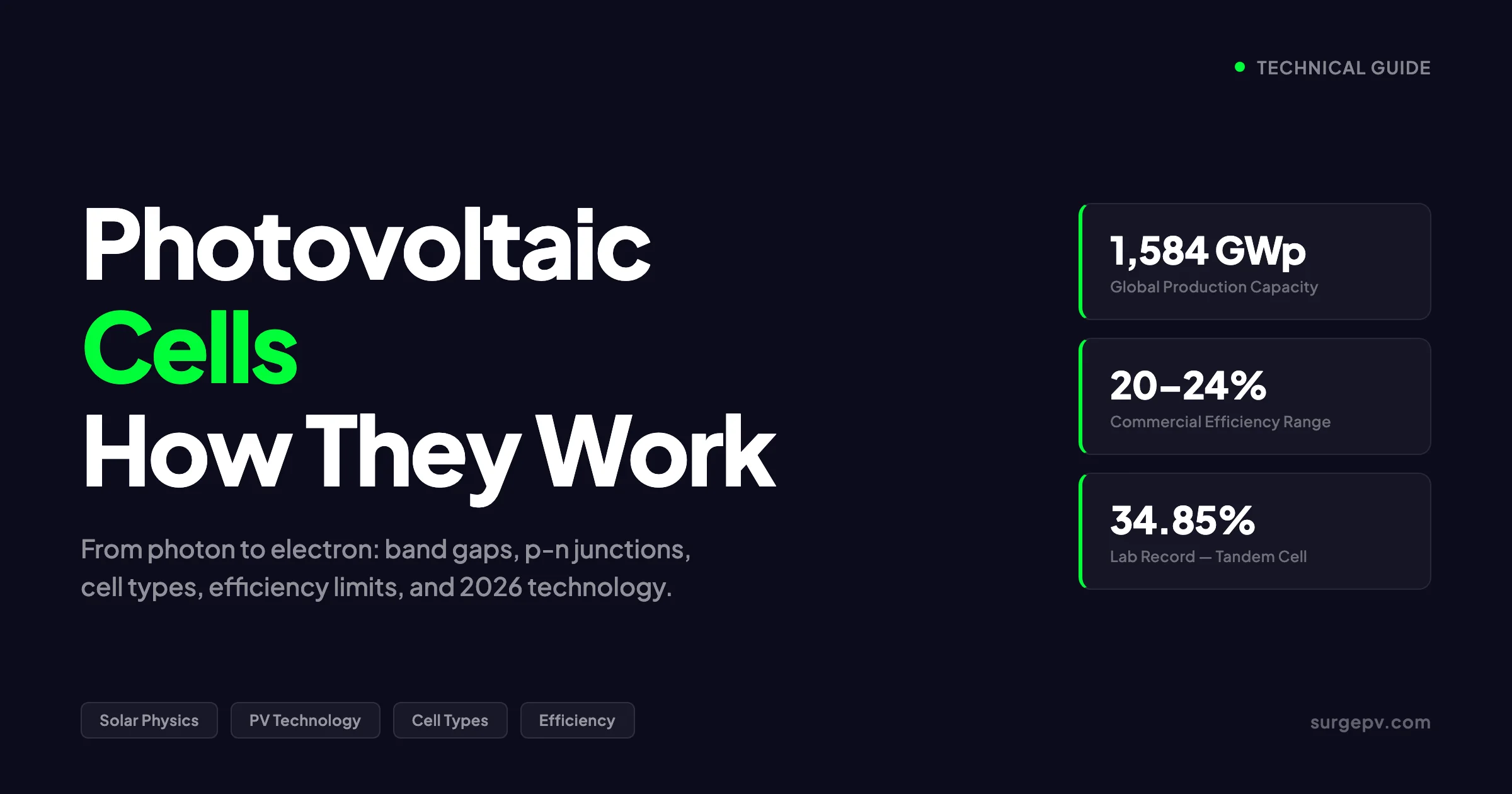
The global photovoltaic cell production capacity reached 1,584 GWp by the end of 2025, according to the European PV Journal . IRENA reports that solar PV accounted for approximately 75% of all renewable capacity additions in 2024. The modern photovoltaic cell emerged in 1954 at Bell Labs, where researchers Daryl Chapin, Calvin Fuller, and Gerald Pearson created the first silicon solar cell with 6% efficiency.
Every solar installation starts with a single semiconductor sandwich no thicker than a human hair. That sandwich — a photovoltaic cell — is where sunlight becomes electricity. Understanding how it works is not academic trivia for installers. It is the difference between selling a system based on generic claims and explaining to a homeowner exactly why their 400 W panel will produce 340 W in year 20, or why south-facing arrays outperform east-west splits by 15-25% in most European climates. Accurate solar software models these real-world effects so installers can size systems correctly and quote with confidence. Also see: European Solar Incentives.
The global photovoltaic cell production capacity reached 1,584 GWp by the end of 2025, according to the European PV Journal . IRENA reports that solar PV accounted for approximately 75% of all renewable capacity additions in 2024. For Global-specific compliance details, see Global net-metering-by-country. For Global-specific compliance details, see Global solar-permitting-speed-by-country.
The global photovoltaic cell production capacity reached 1,584 GWp by the end of 2025, according to the European PV Journal. IRENA reports that solar PV accounted for approximately 75% of all renewable capacity additions in 2024. The market value exceeded $206 billion in 2026. Behind those numbers is a manufacturing and physics story that has not changed in its fundamentals since Edmond Becquerel discovered the photovoltaic effect in 1839, but has evolved dramatically in its execution.
This guide covers the full picture: the semiconductor physics that makes PV possible, the step-by-step process from photon to electron, every major cell type on the market, efficiency limits and real-world losses, how cells are manufactured, what degrades them over time, and the 2026 technology market that is shifting from p-type PERC to n-type TOPCon and HJT architectures.
TL;DR — Photovoltaic Cells
Photovoltaic cells convert sunlight into electricity through the photovoltaic effect in semiconductor materials. Silicon cells with a p-n junction dominate the market, producing 0.5-0.6 V each. Commercial monocrystalline cells reach 20-24% efficiency. The global production capacity is 1,584 GWp. N-type cells (TOPCon, HJT) are replacing p-type PERC as the dominant architecture in 2026. Perovskite tandem cells have reached 34.85% in the lab and are entering commercial production.
In this guide:
- The photovoltaic effect explained: from Becquerel 1839 to modern semiconductors
- Band gap physics and why silicon won the materials race
- The p-n junction: how an electric field separates charges
- Step-by-step: photon to electron to usable DC power
- Every major cell type compared: monocrystalline, polycrystalline, thin-film, perovskite, tandem
- Efficiency limits: the Shockley-Queisser boundary and where energy is lost
- Temperature coefficients and real-world performance gaps
- Manufacturing: from quartz sand to finished module
- Degradation mechanisms every installer should understand
- 2026 technology shifts: n-type, bifacial, perovskite tandems Also see: Us Residential Solar Market Trends 2026.
What Is the Photovoltaic Effect?
The photovoltaic effect is the direct conversion of light energy into electrical energy within a semiconductor material. It is not the same as photosynthesis, which stores chemical energy. It is not the same as solar thermal, which converts light to heat. The photovoltaic effect produces electricity immediately, with no moving parts, no fuel, and no emissions.
Edmond Becquerel, a French physicist, first observed the effect in 1839 while experimenting with an electrolytic cell made of platinum electrodes immersed in a conductive solution. When exposed to light, the cell produced a small voltage. The discovery sat largely unused for over a century. For France-specific information, see Agricultural Solar Case Study.
The modern photovoltaic cell emerged in 1954 at Bell Labs, where researchers Daryl Chapin, Calvin Fuller, and Gerald Pearson created the first silicon solar cell with 6% efficiency. Their goal was to power remote telephone relay stations. Within four years, silicon solar cells were powering satellites — the Vanguard 1 satellite, launched in 1958, carried a small PV array and remains in orbit today. The U.S. Department of Energy maintains a detailed overview of how these early discoveries evolved into today’s commercial technology.
Why Semiconductors?
The photovoltaic effect only works in materials with a specific electronic structure called a band gap. Metals conduct electricity too well — their electrons are already free, so light cannot create additional useful charge separation. Insulators have band gaps that are too wide — photons from sunlight do not carry enough energy to free electrons. Semiconductors sit in the middle. Their band gap is narrow enough that visible light photons can excite electrons across it, but wide enough that the electrons remain bound in the dark.
Silicon has a band gap of approximately 1.1 electron volts (eV). This is not the theoretically optimal value — that would be around 1.34 eV — but silicon won the commercial race because it is the second most abundant element in the Earth’s crust, it can be refined to extreme purity, and decades of semiconductor manufacturing experience from the microelectronics industry transferred directly to solar cell production.
Pro Tip
When explaining the photovoltaic effect to a homeowner, use the staircase analogy. Electrons sit on a lower step (the valence band). A photon of light gives an electron enough energy to jump to a higher step (the conduction band). The p-n junction is like a one-way gate that pushes electrons down a wire before they can fall back. No light, no jump. No junction, no usable current.
The Physics of a PV Cell: Band Gap and the P-N Junction
To understand how a photovoltaic cell works, you need to understand two linked concepts: the band gap of the semiconductor material and the p-n junction that creates the electric field inside the cell.
Energy Bands and the Band Gap
In a solid material, electrons occupy discrete energy levels. In a semiconductor, these levels group into two primary bands separated by a forbidden region:
| Band | Description |
|---|---|
| Valence band | Lower energy level where electrons are bound to atoms and cannot move freely |
| Conduction band | Higher energy level where electrons are free to move and conduct electricity |
| Band gap (Eg) | The energy difference between the valence and conduction bands |
The band gap is measured in electron volts (eV). For silicon, Eg equals approximately 1.1 eV. For gallium arsenide (GaAs), a high-efficiency material used in space applications, Eg equals 1.43 eV. For cadmium telluride (CdTe), a thin-film material, Eg equals 1.5 eV.
When a photon strikes the semiconductor, one of three things happens:
-
Photon energy is below the band gap (E_photon < Eg). The photon passes through the material unabsorbed. This is transparency loss. For silicon, photons with wavelengths longer than approximately 1,100 nm (infrared) pass through without generating electricity.
-
Photon energy equals the band gap (E_photon = Eg). The photon is absorbed, and its energy is just enough to push an electron from the valence band to the conduction band. This is the ideal case — all photon energy converts to electrical potential.
-
Photon energy exceeds the band gap (E_photon > Eg). The photon is absorbed, but the electron is pushed well above the conduction band minimum. The electron quickly relaxes to the bottom of the conduction band, and the excess energy is lost as heat. This is called thermalization loss. It accounts for roughly 33% of all energy loss in a silicon cell.
This trade-off is fundamental. A smaller band gap absorbs more photons but loses more energy to thermalization. A larger band gap retains more voltage per photon but absorbs fewer photons overall. William Shockley and Hans Queisser calculated in 1961 that the optimal band gap for a single-junction cell under standard sunlight is approximately 1.34 eV, yielding a maximum theoretical efficiency of about 33%.
Doping: Creating N-Type and P-Type Silicon
Pure silicon is a poor conductor. Each silicon atom has four electrons in its outer shell and forms covalent bonds with four neighboring atoms. At room temperature, almost all electrons remain locked in these bonds. To make silicon useful for photovoltaics, manufacturers introduce small amounts of other elements in a process called doping.
N-type doping adds elements with five outer-shell electrons, such as phosphorus or arsenic. Four of these electrons form bonds with neighboring silicon atoms. The fifth electron is loosely bound and becomes a free charge carrier at room temperature. N-type silicon has an excess of negative charge carriers (electrons).
P-type doping adds elements with three outer-shell electrons, such as boron or gallium. These atoms form bonds with three neighboring silicon atoms, leaving one bond incomplete. This missing electron behaves as a positive charge carrier called a hole. P-type silicon has an excess of positive charge carriers (holes).
The doping concentration is extremely low — typically one dopant atom per million silicon atoms — but it is enough to dramatically increase conductivity.
The P-N Junction and Built-In Electric Field
A photovoltaic cell is essentially a large-area diode formed by joining a thin layer of n-type silicon to a thicker layer of p-type silicon. At the boundary between them — the p-n junction — something critical happens.
Electrons from the n-side diffuse into the p-side, where they recombine with holes. Holes from the p-side diffuse into the n-side, where they recombine with electrons. This diffusion leaves behind positively charged donor ions on the n-side of the junction and negatively charged acceptor ions on the p-side. The region around the junction becomes depleted of free charge carriers — hence the name depletion region.
These fixed ions create an electric field that points from the n-side to the p-side. This built-in electric field acts as a one-way barrier. It opposes further diffusion of electrons and holes across the junction. The result is a built-in voltage of approximately 0.6 to 0.7 volts for silicon at room temperature.
This electric field is the engine of the photovoltaic cell. Without it, photo-generated electrons and holes would simply recombine within microseconds, producing heat rather than electricity. The field separates the charges and drives them in opposite directions, creating a usable voltage across the cell.
Why Silicon Uses a P-N Junction
Some texts describe the photovoltaic effect as simply “light knocking electrons loose.” That is incomplete. Light does knock electrons loose in many materials — that is the photoelectric effect, discovered by Heinrich Hertz and explained by Albert Einstein. But the photoelectric effect alone does not produce a sustained electric current. The electrons fall back into their atoms almost immediately.
The p-n junction solves this problem. It provides a permanent, built-in electric field that separates photo-generated electrons and holes before they can recombine. It is the combination of photon absorption and charge separation that makes the photovoltaic effect useful for power generation.
Step by Step: How a Photovoltaic Cell Generates Electricity
The process from sunlight to electricity follows six distinct steps inside every photovoltaic cell. Understanding these steps helps installers diagnose underperformance, explain system behavior to customers, and select appropriate modules for specific climates.
Step 1: Photon Enters the Cell
Sunlight reaches the cell as photons — packets of electromagnetic energy with wavelengths ranging from approximately 300 nm (ultraviolet) to 2,500 nm (infrared). Only photons with energy at or above the band gap can generate electricity. For silicon, this means wavelengths shorter than approximately 1,100 nm.
Before reaching the semiconductor, photons pass through several layers:
| Layer | Function | Thickness |
|---|---|---|
| Tempered glass | Physical protection, transmits >91% of light | 3-4 mm |
| Ethylene vinyl acetate (EVA) | Encapsulant, bonds layers, prevents moisture | 0.5 mm |
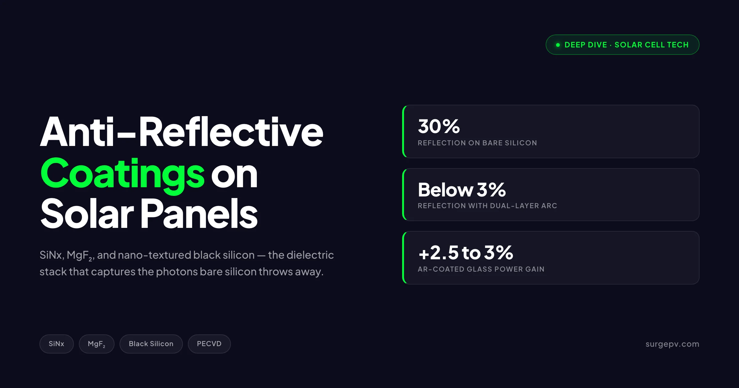
| Anti-reflective coating | Reduces reflection from 30% to under 5% | under 100 nm |
| Front metal grid | Collects electrons; shades under 5% of cell area | 10-30 um |
The anti-reflective coating is critical. Bare silicon reflects approximately 30% of incident light. A silicon nitride (SiNx) anti-reflective coating reduces this to below 5%, dramatically increasing the number of photons that enter the cell.
Step 2: Photon Is Absorbed
Once inside the semiconductor, a photon with sufficient energy is absorbed by the silicon lattice. The energy transfers to an electron in the valence band, exciting it across the band gap into the conduction band. This creates an electron-hole pair — a free negative charge (the electron) and a free positive charge (the hole left behind).
The absorption depth depends on photon wavelength. High-energy photons (blue light, ~450 nm) are absorbed within the first few micrometers of silicon. Lower-energy photons (red light, ~700 nm) travel 10-20 micrometers before absorption. Near-infrared photons near the band gap edge may travel 100+ micrometers. This is why the p-type base layer in a typical silicon cell is 150-200 micrometers thick — it needs enough material to absorb the longer-wavelength photons. For the latest details on Italy, see Commercial Rooftop Solar Case Study Italy.
Step 3: Charge Separation
The electron-hole pair is created in or near the depletion region. The built-in electric field at the p-n junction exerts force on both charges: it pushes the electron toward the n-side and the hole toward the p-side. This separation happens in picoseconds — trillionths of a second.
If the electron and hole are created far from the junction, they must diffuse through the silicon before reaching the electric field. During this diffusion, they can recombine — the electron falls back into a hole, releasing energy as heat or light. The minority carrier lifetime — how long an electron survives in p-type material before recombining — is a key quality metric for solar cell silicon. High-purity silicon has minority carrier lifetimes of hundreds of microseconds. Low-purity silicon may have lifetimes below 10 microseconds, leading to significant recombination losses.
Step 4: Current Collection
Once separated, electrons accumulate in the n-type layer and holes accumulate in the p-type layer. This charge separation creates a voltage difference across the cell — approximately 0.5 to 0.6 volts for a typical silicon cell under standard illumination.
Metal contacts on the front and rear of the cell provide a path for electrons to flow through an external circuit. The front contact is a grid of thin silver fingers that minimizes shading while providing low-resistance collection. The rear contact is a continuous aluminum layer that covers most of the back surface.
Step 5: External Circuit
When the cell is connected to a load — a light bulb, a battery, an inverter — electrons flow from the n-side through the external circuit, do electrical work, and return to the p-side where they recombine with holes. This flow of electrons is direct current (DC) electricity.
The current a cell produces is proportional to the light intensity. Double the light, double the current. The voltage changes only slightly with light intensity — it is primarily determined by the semiconductor band gap and temperature.
Step 6: DC to AC Conversion
Most electrical devices and the grid operate on alternating current (AC). An inverter converts the DC electricity from the solar cells into AC electricity. Modern string inverters achieve conversion efficiencies of 97-99%. Solar design software models the full DC-to-AC conversion chain, including inverter clipping, mismatch losses, and temperature derating.
Why Metal Contacts Matter
The grid pattern on the front of a solar cell is not decorative. It is an electrical engineering compromise. Thicker fingers would collect electrons more efficiently but would block more light. Thinner fingers block less light but have higher electrical resistance. Modern cells use screen-printed silver fingers approximately 30-40 micrometers wide, with busbars (thicker collector lines) running horizontally.
Back contact cells, such as IBC (interdigitated back contact) and HJT architectures, move all contacts to the rear surface. This eliminates front shading entirely and can add 1-2 percentage points of absolute efficiency. The trade-off is more complex manufacturing.
From Cell to Module to Array
A single silicon cell produces approximately 0.5 V and 6-9 A under standard test conditions — roughly 3-5 watts. That is not enough for most applications.
Cells are connected in series to increase voltage. A typical 60-cell module strings 60 cells together, producing approximately 30-40 V open-circuit. Modules are connected in strings to reach inverter input voltages of 400-1,000 V. Strings are connected in parallel to increase current. The complete assembly from cells to array multiplies power from a few watts per cell to kilowatts or megawatts per installation.
Types of Photovoltaic Cells: A Complete Comparison
Photovoltaic cells are grouped into three generations based on their maturity and underlying technology. Each generation has distinct efficiency, cost, and application profiles.
First Generation: Crystalline Silicon
Crystalline silicon cells account for approximately 95% of the global solar market in 2026. They are mature, reliable, and manufactured at massive scale.
Monocrystalline Silicon
Monocrystalline cells are cut from a single, continuous silicon crystal. The manufacturing process begins with the Czochralski method: a seed crystal is dipped into molten high-purity silicon and slowly rotated and pulled upward, forming a cylindrical ingot. This ingot is sliced into thin wafers.
| Parameter | Value |
|---|---|
| Typical efficiency | 20-24% (commercial modules) |
| Cell color | Uniform dark blue or black |
| Wafer thickness | 160-180 micrometers |
| Temperature coefficient | -0.30 to -0.40% per degree C |
| Degradation rate | 0.30-0.55% per year |
| Cost | Higher than polycrystalline |
Monocrystalline cells have higher efficiency because the single-crystal structure has fewer defects and grain boundaries where electrons can recombine. The uniform appearance comes from the consistent crystal orientation across the entire wafer.
In 2026, monocrystalline technology has almost entirely displaced polycrystalline in new production. Module efficiencies of 21-22% are standard for residential modules, with premium modules reaching 23-24%.
Polycrystalline Silicon
Polycrystalline cells are made by pouring molten silicon into a square mold and allowing it to cool and solidify. The resulting block contains multiple crystal grains oriented in different directions. The block is then sliced into wafers.
| Parameter | Value |
|---|---|
| Typical efficiency | 15-18% (commercial modules) |
| Cell color | Blue with visible speckled grain pattern |
| Wafer thickness | 180-200 micrometers |
| Temperature coefficient | -0.40 to -0.50% per degree C |
| Degradation rate | 0.50-0.80% per year |
| Cost | Lower than monocrystalline |
The grain boundaries in polycrystalline silicon act as recombination sites, reducing efficiency. However, the manufacturing process is simpler and cheaper because it skips the slow crystal-pulling step. Polycrystalline modules dominated the market from 2010 to 2020 due to their lower cost per watt.
By 2026, polycrystalline production has nearly stopped. The cost gap between mono and poly has closed as monocrystalline manufacturing scaled up, and the efficiency advantage of monocrystalline (4-6 absolute percentage points) became too significant to ignore.
Second Generation: Thin-Film
Thin-film cells deposit photovoltaic material as a thin layer on a substrate such as glass, plastic, or metal. The active layer is typically 1-10 micrometers thick — 20-100 times thinner than crystalline silicon wafers.
Cadmium Telluride (CdTe)
CdTe is the most commercially successful thin-film technology, dominated by First Solar. It has a near-optimal band gap of 1.5 eV and can be deposited quickly using vapor transport deposition.
| Parameter | Value |
|---|---|
| Typical efficiency | 16-19% (modules) |
| Band gap | 1.5 eV |
| Temperature coefficient | -0.25 to -0.30% per degree C |
| Key advantage | Better high-temperature performance than silicon |
| Key concern | Cadmium is toxic; tellurium is rare |
CdTe modules perform better than silicon in hot climates because of their lower temperature coefficient. However, cadmium toxicity and limited tellurium supply constrain market growth.
Copper Indium Gallium Selenide (CIGS)
CIGS cells use a quaternary compound semiconductor with a tunable band gap. They can be deposited on flexible substrates, enabling building-integrated and portable applications.
| Parameter | Value |
|---|---|
| Typical efficiency | 15-20% (modules) |
| Band gap | Tunable, 1.0-1.7 eV |
| Temperature coefficient | -0.30 to -0.40% per degree C |
| Key advantage | Flexible substrate compatibility |
| Key concern | Complex manufacturing, indium scarcity |
CIGS lab cells have reached 23.4% efficiency, but manufacturing consistency remains a challenge. The technology is used in niche applications such as portable chargers, building-integrated photovoltaics, and space-constrained installations.
Amorphous Silicon (a-Si)
Amorphous silicon has no crystal structure. It can be deposited at low temperatures on various substrates including plastic and glass. However, its efficiency is low, and it suffers from light-induced degradation (the Staebler-Wronski effect).
| Parameter | Value |
|---|---|
| Typical efficiency | 6-8% (single junction) |
| Band gap | 1.7 eV |
| Key advantage | Very low material use, flexible deposition |
| Key concern | Low efficiency, light-induced degradation |
Amorphous silicon is rarely used as a standalone technology today. It is occasionally used in multi-junction configurations or in consumer electronics such as calculators.
Third Generation: Emerging Technologies
Third-generation cells aim to break through the Shockley-Queisser limit using novel materials and architectures.
Perovskite Solar Cells
Perovskites are a family of materials with a specific crystal structure (ABX3). The most common solar perovskite is methylammonium lead iodide. Perovskites have a tunable band gap, can be solution-processed at low temperatures, and have shown the fastest efficiency improvement of any photovoltaic technology.
| Parameter | Value |
|---|---|
| Lab efficiency | 26.1% (single junction, certified) |
| Tandem with silicon | 34.85% (LONGi, NREL-certified, 2025) |
| Band gap | Tunable, 1.2-2.3 eV |
| Key advantage | Low-cost processing, tunable band gap |
| Key concern | Stability (moisture, heat, UV), lead content |
Perovskite cells have improved from 3.8% efficiency in 2009 to over 26% in 2025 — a rate of progress unmatched in photovoltaic history. The tunable band gap makes them ideal for tandem configurations with silicon.
The stability challenge is significant. Early perovskite cells degraded within hours of exposure to moisture and UV light. By 2026, encapsulated perovskite cells demonstrate thousands of hours of stability under standard test conditions, but long-term field data is still limited.
Heterojunction with Intrinsic Thin Layer (HJT)
HJT cells combine crystalline silicon with thin layers of amorphous silicon on both sides. The amorphous silicon layers passivate the silicon surface, reducing recombination and enabling higher voltages.
| Parameter | Value |
|---|---|
| Typical efficiency | 24-26% (modules) |
| Temperature coefficient | -0.24 to -0.26% per degree C |
| Key advantage | High efficiency, excellent temperature performance |
| Key concern | Complex manufacturing, silver paste usage |
HJT cells achieve higher open-circuit voltages than conventional silicon cells — typically 740-750 mV per cell versus 680-700 mV for PERC. The lower temperature coefficient makes HJT particularly attractive for hot climates. Major manufacturers including REC, Maxeon, and several Chinese producers have scaled HJT production in 2025-2026.
Tunnel Oxide Passivated Contact (TOPCon)
TOPCon cells add an ultra-thin tunnel oxide layer and a doped polysilicon layer to the rear of a conventional silicon cell. This creates a passivated contact that reduces recombination while maintaining good electrical conductivity.
| Parameter | Value |
|---|---|
| Typical efficiency | 24-26% (modules) |
| Temperature coefficient | -0.30 to -0.32% per degree C |
| Key advantage | High efficiency, compatible with existing PERC lines |
| Key concern | Complex boron doping, process control |
TOPCon is the fastest-growing cell architecture in 2026 because it can be manufactured on upgraded PERC production lines. JinkoSolar, LONGi, and Trina Solar have all announced massive TOPCon capacity expansions. Runergy achieved a 26.6% efficiency record for an M10-sized TOPCon cell in 2025, entering the NREL chart as the first Chinese company in the single-crystalline silicon category.
Multi-Junction and Tandem Cells
Multi-junction cells stack two or more p-n junctions with different band gaps on top of each other. High-energy photons are absorbed by the top junction. Lower-energy photons pass through to the bottom junction. This captures more of the solar spectrum than any single-junction cell.
| Configuration | Record Efficiency | Application |
|---|---|---|
| III-V triple junction (concentrated) | 47.6% | Space, concentrator systems |
| Perovskite-silicon tandem | 34.85% | Emerging commercial |
| Perovskite-perovskite tandem | 29.4% | Research |
Space satellites use III-V triple-junction cells (gallium indium phosphide / gallium arsenide / germanium) because the cost per watt is irrelevant and efficiency per unit area is critical. Concentrator photovoltaic systems use similar cells with mirrors or lenses that focus sunlight 500-1,000 times, achieving efficiencies above 47%. For the latest details on Germany, see Community Solar Projects Germany. See Community Solar Business Model for detailed guidance.
For terrestrial applications, perovskite-silicon tandems are the most promising. Oxford PV shipped the first commercial perovskite-silicon tandem modules in September 2024 with 24.5% module efficiency. Hanwha Qcells announced a 28.6% M10-sized cell in December 2024 targeting mass production by 2027.
Understanding Solar Cell Efficiency: Limits and Losses
Solar cell efficiency is the percentage of incoming solar energy that converts to electrical energy. The best commercial silicon modules reach 20-24%. The best lab cells exceed 33%. Understanding why the gap exists — and why even 33% is a hard ceiling — is essential for anyone who specifies or installs solar equipment.
The Shockley-Queisser Limit
In 1961, physicists William Shockley and Hans Queisser calculated the theoretical maximum efficiency for a single-junction solar cell under standard sunlight. Their analysis considered two fundamental constraints:
-
Sub-bandgap photons cannot be absorbed. Photons with energy below the band gap pass through the cell unabsorbed. For silicon, this means all infrared photons with wavelengths longer than 1,100 nm are lost.
-
Thermalization wastes excess energy. Photons with energy above the band gap excite electrons far above the conduction band minimum. The electrons quickly relax, losing the excess energy as heat.
The Shockley-Queisser limit for a single-junction cell with optimal band gap is approximately 33.7%. For silicon, with its 1.1 eV band gap, the limit is approximately 29.4%. No single-junction silicon cell can ever exceed this value, regardless of manufacturing perfection.
Where Does the Energy Go? Breaking Down the Losses
A typical commercial silicon cell converts approximately 20% of incoming solar energy to electricity. The remaining 80% is lost through several mechanisms:
| Loss Mechanism | Approximate Energy Lost | Cause |
|---|---|---|
| Sub-bandgap transmission | ~19% | Photons with E < Eg pass through unabsorbed |
| Thermalization | ~33% | Excess photon energy lost as heat |
| Recombination | ~3-8% | Electron-hole pairs recombine before collection |
| Reflection | ~1-3% | Light reflected from cell surface |
| Grid shading | ~3-5% | Front metal contacts block light |
| Electrical resistance | ~1-2% | Resistance in contacts, busbars, and interconnects |
| Fill factor loss | ~2-4% | Non-ideal diode behavior at high current |
The largest single loss is thermalization. A blue photon at 450 nm carries approximately 2.75 eV of energy. In silicon, only 1.1 eV is needed to cross the band gap. The remaining 1.65 eV — roughly 60% of the photon’s energy — becomes heat. This is why solar cells warm up in sunlight and why cooling matters for performance.
Temperature Coefficients and Real-World Performance
Solar cell efficiency decreases as temperature increases. This is counterintuitive — more sunlight should mean more power — but the physics is clear. As temperature rises:
- The band gap narrows, reducing the cell voltage
- Carrier lifetime decreases, increasing recombination
- The built-in electric field weakens slightly
The temperature coefficient quantifies this effect. Most silicon cells lose 0.3-0.5% of their rated output for every degree Celsius above 25 degrees C (standard test condition temperature).
| Cell Technology | Temperature Coefficient (per degree C) | Power Loss at 65 degrees C vs. 25 degrees C |
|---|---|---|
| Monocrystalline PERC | -0.35% | 14% |
| Monocrystalline TOPCon | -0.30% | 12% |
| HJT | -0.25% | 10% |
| CdTe | -0.28% | 11% |
A module rated at 400 W at 25 degrees C may produce only 340-350 W on a 65-degree C rooftop in summer. This is why solar design software includes temperature derating in production estimates, and why installers should account for local climate when predicting annual yield.
Pro Tip
In hot climates, prioritize modules with low temperature coefficients. An HJT module with a -0.25% per degree C coefficient will produce approximately 4% more annual energy than a standard PERC module with -0.40% per degree C in a desert environment where module temperatures regularly exceed 70 degrees C. That 4% compounds over 25 years.
Measuring Efficiency: Standard Test Conditions
Solar cell efficiency is measured under Standard Test Conditions (STC) to enable fair comparison:
| Parameter | STC Value |
|---|---|
| Irradiance | 1,000 W per m² |
| Cell temperature | 25 degrees C |
| Air mass | 1.5 (sunlight passing through 1.5 times the thickness of Earth’s atmosphere) |
| Spectrum | ASTM G173 (global tilted) |
STC represents ideal laboratory conditions, not real-world rooftop performance. On an actual installation, irradiance varies from 0 to 1,200+ W per m², cell temperatures range from below freezing to above 80 degrees C, and spectrum shifts with time of day and atmospheric conditions. Solar shadow analysis software accounts for these variations when modeling annual production.
The nameplate wattage on a module — 400 W, 550 W, 600 W — is the power output under STC. Actual output will be lower for most of the year due to temperature, soiling, and sub-ideal irradiance.
From Laboratory to Rooftop: Manufacturing a PV Cell
Understanding how photovoltaic cells are manufactured helps installers appreciate quality differences between modules and explain warranty terms to customers.
Polysilicon Production
The process begins with quartz sand (silicon dioxide, SiO2), which is reduced to metallurgical-grade silicon in an electric arc furnace at approximately 2,000 degrees C. This metallurgical silicon is approximately 98-99% pure — not nearly pure enough for solar cells.
The Siemens process purifies silicon to 99.9999999% (nine nines, or “9N”) purity. Trichlorosilane gas is deposited onto thin silicon rods in a chemical vapor deposition reactor. The resulting polysilicon chunks are the raw material for crystalline silicon cells. Global polysilicon production capacity was approximately 3.7 million tonnes by end of 2025 — enough for roughly 1,763 GWp of cell production.
Ingot and Wafer Formation
For monocrystalline cells, the Czochralski process grows a single crystal ingot. A seed crystal is dipped into molten polysilicon and slowly pulled upward while rotating. The process takes 24-48 hours and produces a cylindrical ingot 200-300 mm in diameter and several meters long.
The ingot is sliced into thin wafers using diamond wire saws. Each wafer is 160-180 micrometers thick. Wire sawing produces kerf loss — approximately 150-200 micrometers of silicon turns into dust per cut. Reducing kerf loss is a major focus of manufacturing R&D.
For polycrystalline cells, molten silicon is poured into a square mold and directionally solidified. The resulting block is sliced into square wafers without the cylindrical shape loss of the Czochralski process.
Cell Fabrication Steps
Wafer to finished cell involves several processing steps:
-
Texturing: The wafer surface is etched to create microscopic pyramids. These pyramids trap light through multiple internal reflections, increasing absorption.
-
Diffusion: The wafer is heated in a furnace with phosphorus-containing gas. Phosphorus diffuses into the surface, creating a thin n-type layer on top of the p-type wafer. This forms the p-n junction.
-
Edge isolation: The diffusion process coats the wafer edges with n-type material, which would short-circuit the cell. A laser or chemical process removes this edge coating.
-
Anti-reflective coating: Silicon nitride (SiNx) is deposited using plasma-enhanced chemical vapor deposition. This coating reduces reflection from 30% to below 5%.
-
Contact formation: Silver paste is screen-printed on the front surface in a grid pattern. Aluminum paste is printed on the rear. The wafer is fired in a furnace at approximately 800 degrees C, which sinters the metal into the silicon.
-
Testing and sorting: Each cell is tested under a solar simulator. Cells are sorted into efficiency bins and matched for module assembly.
Module Assembly
Finished cells are assembled into modules:
-
Cell interconnection: Cells are soldered together in series using copper ribbons. A 60-cell module has 59 solder joints connecting the cells.
-
Lamination: The cell string is placed between layers of EVA encapsulant, covered with tempered glass on top and a polymer backsheet on the bottom. The stack is heated and pressed in a vacuum laminator, which melts the EVA and bonds all layers together.
-
Framing: An aluminum frame is attached for mechanical protection and mounting compatibility.
-
Junction box: A junction box is attached to the rear, containing bypass diodes that prevent hot spots if part of the module is shaded.
-
Final testing: The completed module is tested under a flash simulator to verify power output, current-voltage characteristics, and insulation resistance.
Real-World Performance: What Installers Need to Know
A module’s nameplate rating is a starting point, not a guarantee. Several factors reduce real-world performance below the STC value.
Degradation Rates Over Time
All photovoltaic cells degrade gradually. The rate depends on technology, climate, and manufacturing quality.
| Technology | First-Year Degradation | Annual Degradation (Years 2-25) |
|---|---|---|
| Monocrystalline PERC | 1.0-2.0% | 0.40-0.55% |
| Monocrystalline TOPCon | 1.0-1.5% | 0.30-0.40% |
| HJT | 1.0-1.5% | 0.25-0.35% |
| CdTe | 0.5-1.0% | 0.40-0.50% |
A 400 W monocrystalline PERC module with 1.5% first-year degradation and 0.50% annual degradation will produce approximately 345 W in year 25. A 25-year warranty typically guarantees at least 80-85% of original output at the end of the warranty period.
Light-Induced Degradation (LID)
LID affects boron-doped crystalline silicon cells. When first exposed to sunlight, boron-oxygen complexes form in the silicon lattice. These complexes act as recombination centers, reducing carrier lifetime and efficiency. The effect stabilizes after the first few hundred hours of exposure, with total loss of 1-3%.
Modern p-type PERC cells use regeneration techniques that partially reverse LID. N-type cells, which use phosphorus-doped silicon rather than boron-doped silicon, are immune to LID. This is one reason n-type technologies (TOPCon, HJT) are displacing p-type PERC.
Potential-Induced Degradation (PID)
PID occurs when high voltage between the cell and the module frame drives ion migration through the encapsulant. Sodium ions from the glass migrate to the cell surface, where they create shunt paths that bypass the p-n junction. PID can cause 5-30% power loss.
PID is most severe in hot, humid climates with systems operating at high string voltages (800-1,000 V or 1,500 V). Mitigation strategies include using PID-resistant encapsulants, grounding the module frame, and operating at lower voltages.
Soiling and Shading Impact
Dust, pollen, bird droppings, and pollution reduce the light reaching the cell surface. Soiling losses vary dramatically by location:
| Environment | Typical Soiling Loss |
|---|---|
| Clean temperate climate | 2-5% annually |
| Agricultural area | 5-10% annually |
| Urban / industrial | 5-15% annually |
| Desert | 20-40% without cleaning |
Shading has a disproportionate impact because modern modules use bypass diodes that isolate shaded sections. A single shaded cell in a string can reduce the entire string’s output, though bypass diodes limit the loss to approximately one-third of the module’s power per shaded section.
solar shadow analysis software models shading losses using 3D terrain and building data, helping installers predict real-world yield before construction.
Mismatch Losses
Cells in a module and modules in a string are never perfectly identical. Small variations in manufacturing, temperature, and degradation rate create mismatch. A typical mismatch loss of 1-2% is built into production estimates.
Power optimizers and microinverters reduce mismatch by allowing each module to operate at its own maximum power point. This is particularly valuable for installations with partial shading, multiple roof orientations, or modules from different production batches.
2026 Technology Shifts: What Is Changing
The photovoltaic cell market is undergoing its most significant technology transition since the shift from multicrystalline to monocrystalline silicon.
N-Type Cells Replacing P-Type PERC
P-type PERC (Passivated Emitter and Rear Cell) has been the dominant architecture since 2016. It added a dielectric passivation layer to the rear of a standard aluminum back-surface field cell, reducing rear surface recombination and boosting efficiency by 1-2 percentage points.
By 2026, p-type PERC is being phased out. The reasons are clear:
- LID immunity: N-type cells do not suffer boron-oxygen LID
- Higher efficiency potential: N-type silicon has longer minority carrier lifetimes
- Lower degradation: N-type cells degrade more slowly over 25 years
- Bifacial compatibility: N-type architectures are inherently better suited to bifacial designs
TOPCon and HJT are the leading n-type contenders. Industry analysts project that n-type cells will account for over 70% of global production by 2027, up from approximately 25% in 2024.
| Architecture | 2024 Market Share | 2026 Market Share (Projected) |
|---|---|---|
| P-type PERC | ~70% | ~30% |
| N-type TOPCon | ~15% | ~40% |
| N-type HJT | ~5% | ~15% |
| Other (thin-film, etc.) | ~10% | ~15% |
Bifacial Modules Going Mainstream
Bifacial modules generate electricity from both front and rear surfaces. Light reflected from the ground, roof, or water reaches the rear surface and generates additional current. Bifacial gain — the extra energy from the rear side — ranges from 5-30% depending on albedo (surface reflectivity) and installation geometry. Read Bifacial Solar Panel Design Guide for a complete walkthrough.
| Surface | Albedo | Typical Bifacial Gain |
|---|---|---|
| Grass | 0.15-0.25 | 5-10% |
| Concrete | 0.30-0.40 | 10-15% |
| White membrane roof | 0.60-0.80 | 20-30% |
| Snow | 0.60-0.90 | 25-40% (seasonal) |
Bifacial modules require different modeling than monofacial modules. The rear-side irradiance depends on ground albedo, module height, row spacing, and tilt angle. Solar design software includes bifacial yield models that account for these variables.
Bifacial module market share is projected to reach 50% in 2026, up from 33% in 2023. Most bifacial modules use n-type cells because the rear-side collection benefits from the longer carrier lifetimes of n-type silicon.
Perovskite Tandem Cells Approach Commercialization
Perovskite-silicon tandem cells represent the next major efficiency leap. By stacking a perovskite top cell with a silicon bottom cell, tandems capture more of the solar spectrum than silicon alone.
The commercial timeline has accelerated:
- 2024: Oxford PV ships first commercial perovskite-silicon tandem modules (24.5% module efficiency)
- 2025: LONGi achieves 34.85% cell efficiency (NREL-certified). Hanwha Qcells demonstrates 28.6% M10 cell.
- 2026: Several manufacturers announce pilot production lines. LONGi reports 28.13% silicon cell record and 26.4% module efficiency.
The remaining challenges are stability and manufacturing scale. Perovskite layers must survive 25 years of thermal cycling, humidity, and UV exposure. Current encapsulation solutions show promise but lack the decades of field validation that silicon enjoys.
Efficiency Records and What They Mean
Laboratory efficiency records receive significant media attention, but installers should understand what they represent:
| Record Type | What It Means | Practical Relevance |
|---|---|---|
| Small-area lab cell (under 1 cm²) | Proof of physics; near-perfect material | Low — manufacturing defects scale with area |
| Large-area lab cell (>200 cm²) | Scalable process demonstration | Medium — may reach production in 2-5 years |
| Commercial module | Mass-produced, tested, and shipped | High — this is what installers actually buy |
The jump from lab cell to commercial module typically takes 3-7 years and involves a 3-5 percentage point efficiency reduction. A 33% lab cell might become a 28-29% commercial module. A 28% lab cell might become a 24-25% commercial module.
Design with the Latest Cell Technologies
SurgePV’s solar design platform models n-type TOPCon, HJT, and bifacial modules with accurate temperature coefficients and rear-side gain calculations. Get production estimates that reflect 2026 technology, not outdated assumptions.
Book a DemoNo commitment required · 20 minutes · Live project walkthrough
Conclusion
Photovoltaic cells are semiconductor diodes that convert sunlight into electricity through the photovoltaic effect. The physics has not changed since Becquerel observed it in 1839, but the engineering has transformed a laboratory curiosity into the fastest-growing energy source on Earth.
Three takeaways for solar professionals:
-
Understand the fundamentals. The p-n junction, band gap, and charge separation are not abstract concepts — they explain why cells behave the way they do in heat, shade, and low light. An installer who can explain why a module loses 15% of its output on a 70-degree C rooftop builds more trust than one who quotes efficiency numbers without context.
-
Follow the technology transition. P-type PERC is ending its run. N-type TOPCon and HJT are the present. Perovskite tandems are the near future. Every major manufacturer has announced n-type capacity expansions. Specifying systems with outdated cell technology leaves value on the table for clients.
-
Use accurate modeling. Nameplate wattage under STC is not real-world output. Temperature derating, soiling, shading, degradation, and mismatch all reduce actual production. Solar design software and solar proposal software that account for these factors produce accurate client proposals and reduce post-installation disputes.
Frequently Asked Questions
What is the photovoltaic effect?
The photovoltaic effect is the physical process by which a semiconductor material converts light directly into electricity. Discovered by Edmond Becquerel in 1839, it occurs when photons from sunlight strike a semiconductor and transfer enough energy to free electrons from their atomic bonds, creating an electric current.
How does a p-n junction work in a solar cell?
A p-n junction forms where p-type silicon (doped with boron, creating holes) meets n-type silicon (doped with phosphorus, creating extra electrons). Electrons diffuse across the junction, creating a built-in electric field. When light hits the cell, this field separates photo-generated electron-hole pairs, pushing electrons to the n-side and holes to the p-side, which generates voltage.
What are the main types of photovoltaic cells?
The three main generations are: First generation — crystalline silicon (monocrystalline at 20-24% efficiency, polycrystalline at 15-18%). Second generation — thin-film technologies including CdTe, CIGS, and amorphous silicon (6-22% efficiency). Third generation — emerging technologies such as perovskite, multi-junction tandem cells (lab records above 34%), HJT, and TOPCon architectures.
Why are solar cells limited to about 20-23% efficiency?
Commercial solar cells face several fundamental losses. Photons with energy below the band gap pass through unabsorbed. Photons with excess energy lose the surplus as heat. Some electron-hole pairs recombine before contributing to current. Reflection, shading from metal contacts, and electrical resistance account for additional losses. The theoretical maximum for single-junction silicon is the Shockley-Queisser limit of about 29.4%.
How does temperature affect photovoltaic cell performance?
Higher temperatures reduce PV cell efficiency because the semiconductor band gap narrows, lowering cell voltage. Carrier lifetime decreases, meaning more electrons are lost before contributing to current. Most silicon cells lose 0.3-0.5% of their rated output for every degree Celsius above 25 degrees C. This is why proper ventilation and spacing matter in hot climates.
What is the difference between monocrystalline and polycrystalline solar cells?
Monocrystalline cells are cut from a single silicon crystal, giving them a uniform dark appearance and higher efficiency (20-24%). Polycrystalline cells are made from multiple crystal fragments melted together, resulting in a blue speckled look and lower efficiency (15-18%) but historically lower cost. In 2026, monocrystalline dominates new production as polycrystalline fades from the market.
What are perovskite tandem solar cells?
Perovskite tandem cells stack a perovskite semiconductor layer on top of a silicon cell. The perovskite layer absorbs high-energy photons while letting lower-energy photons pass through to the silicon bottom cell. This captures more of the solar spectrum than silicon alone. Lab records exceeded 34.85% in 2025, and Oxford PV began commercial shipments in late 2024.
How long do photovoltaic cells last?
Most photovoltaic cells carry a 25-year warranty and typically operate for 30+ years. Annual degradation rates range from 0.25-0.8% per year depending on technology and climate. A monocrystalline panel that starts at 400 W may still produce 320-340 W after 25 years. Factors that accelerate degradation include high temperatures, humidity, potential-induced degradation, and mechanical stress.